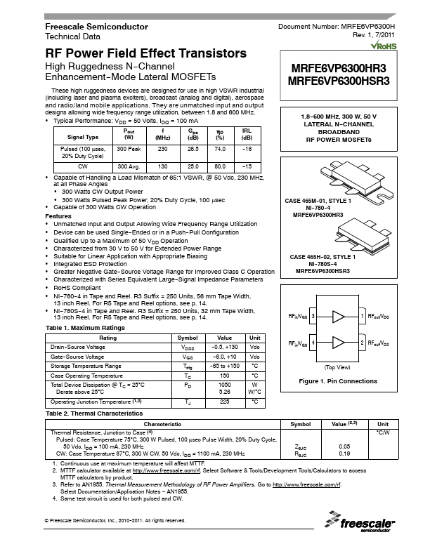
MRFE6VP6300HR3 Description
.DataSheet.co.kr Freescale Semiconductor Technical Data Document Number: 1, 7/2011 RF Power Field Effect Transistors High Ruggedness N--Channel Enhancement--Mode Lateral MOSFETs These high ruggedness devices are designed for use in high VSWR industrial (including laser and plasma exciters), broadcast (analog and digital), aerospace and radio/land mobile applications. They are unmatched input and output designs...
MRFE6VP6300HR3 Key Features
- Unmatched Input and Output Allowing Wide Frequency Range Utilization
- Device can be used Single--Ended or in a Push--Pull Configuration
- Qualified Up to a Maximum of 50 VDD Operation
- Characterized from 30 V to 50 V for Extended Power Range
- Suitable for Linear Application with Appropriate Biasing
- Integrated ESD Protection
- Greater Negative Gate--Source Voltage Range for Improved Class C Operation
- Characterized with Series Equivalent Large--Signal Impedance Parameters
- RoHS pliant
- NI--780--4 in Tape and Reel. R3 Suffix = 250 Units, 56 mm Tape Width, 13 inch Reel. For R5 Tape and Reel options, see p.