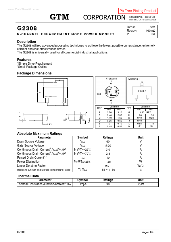
ISSUED DATE :2005/01/17
REVISED DATE :2005/03/22B
Electrical Characteristics(Tj = 25 Unless otherwise specified)
Parameter
Symbol Min. Typ. Max. Unit
Test Conditions
Drain-Source Breakdown Voltage
Breakdown Voltage Temperature Coefficient
Gate Threshold Voltage
Forward Transconductance
Gate-Source Leakage Current
BVDSS
BVDSS / Tj
VGS(th)
gfs
IGSS
60
-
1.0
-
-
-
0.05
-
5.0
-
- V VGS=0, ID=250uA
- V/ Reference to 25 , ID=1mA
3.0 V VDS=VGS, ID=250uA
- S VDS=5V, ID=3A
100 nA VGS= 20V
Drain-Source Leakage Current(Tj=25 )
Drain-Source Leakage Current(Tj=70 )
IDSS
-
-
- 10 uA VDS=60V, VGS=0
- 25 uA VDS=48V, VGS=0
Static Drain-Source On-Resistance RDS(ON)
Total Gate Charge2
Gate-Source Charge
Gate-Drain (“Miller”) Change
Turn-on Delay Time2
Rise Time
Turn-off Delay Time
Fall Time
Input Capacitance
Output Capacitance
Reverse Transfer Capacitance
Qg
Qgs
Qgd
Td(on)
Tr
Td(off)
Tf
Ciss
Coss
Crss
-
-
-
-
-
-
-
-
-
-
-
-
- 160 m VGS=10V, ID=2.0A
- 220
VGS=4.5V, ID=1.7A
6 10
ID=3A
1.6 - nC VDS=48V
3-
VGS=4.5V
6-
VDS=30V
5-
ID=1A
16
-
ns VGS=10V
RG=3.3
3-
RD=30
490 780
55 -
40 -
VGS=0V
pF VDS=25V
f=1.0MHz
Source-Drain Diode
Parameter
Forward On Voltage2
Reverse Recovery Time
Reverse Recovery Charge
Symbol
VSD
Trr
Qrr
Min.
-
-
-
Typ.
-
25
26
Max.
1.2
-
-
Unit Test Conditions
V IS=1.2A, VGS=0V
ns IS=3A, VGS=0V
nC dI/dt=100A/ s
Notes: 1. Pulse width limited by Max. junction temperature.
2. Pulse width 300us, duty cycle 2%.
3. Surface mounted on 1 in2 copper pad of FR4 board;270 /W when mounted on min. copper pad.
2/4