GS66508B
GS66508B is Bottom-side cooled 650V E-mode GaN transistor manufactured by GaN Systems.
Features
- 650 V enhancement mode power transistor
- Bottom-side cooled configuration
- RDS(on) = 50 mΩ
- IDS(max) = 30 A
- Ultra-low FOM die
- Low inductance Ga NPX® package
- Simple gate drive requirements (0 V to 6 V)
- Transient tolerant gate drive (-20 V / +10 V)
- Very high switching frequency (> 10 MHz)
- Fast and controllable fall and rise times
- Reverse conduction capability
- Zero reverse recovery loss
- Small 7.0 x 8.4 mm2 PCB footprint
- Source Sense (SS) pin for optimized gate drive
- Ro HS 3 (6+4) pliant
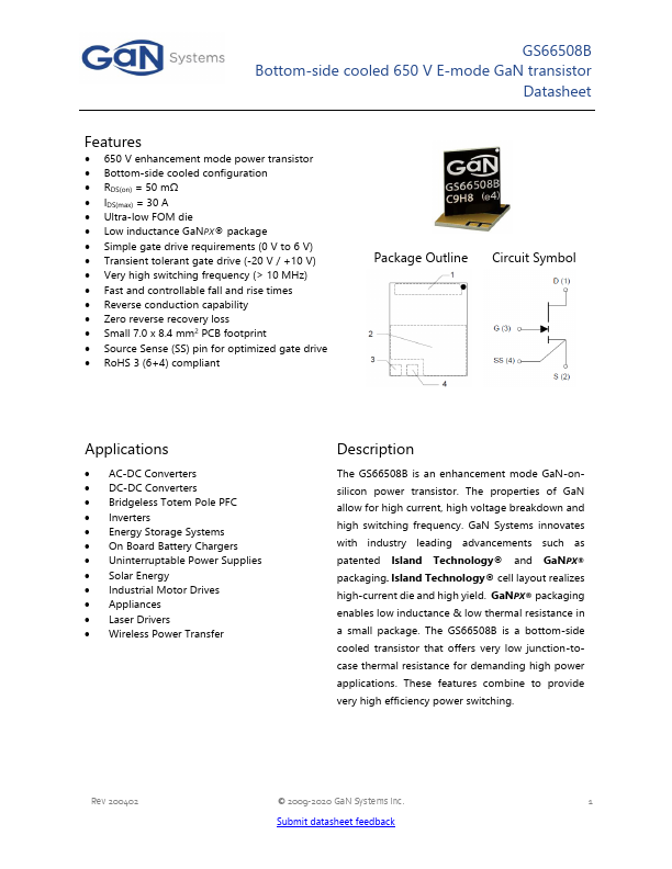
Package Outline Circuit Symbol
Applications
- AC-DC Converters
- DC-DC Converters
- Bridgeless Totem Pole PFC
- Inverters
- Energy Storage Systems
- On Board Battery Chargers
- Uninterruptable Power Supplies
- Solar Energy
- Industrial Motor Drives
- Appliances
- Laser Drivers
- Wireless Power Transfer
Description
The GS66508B is an enhancement mode Ga N-onsilicon power transistor. The properties of Ga N allow for high current, high voltage breakdown and high switching frequency. Ga N Systems innovates with industry leading advancements such as patented Island Technology® and Ga NPX® packaging. Island Technology® cell layout realizes high-current die and high yield. Ga NPX® packaging enables low inductance & low thermal resistance in a small package. The GS66508B is a bottom-side cooled transistor that offers very low junction-tocase thermal resistance for demanding high power applications. These features bine to provide very high efficiency power switching.
Rev 200402
© 2009-2020 Ga N Systems Inc.
Submit datasheet feedback
GS66508B Bottom-side cooled 650 V E-mode Ga N transistor
Absolute Maximum Ratings (Tcase = 25 °C except as noted)
Parameter
Symbol...