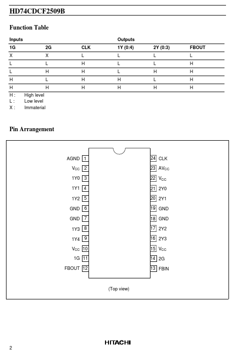
Datasheet4U Logo Datasheet4U.com

HD74CDCF2509B - 140 MHz/ 0 to 85C Operation 3.3-V Phase-lock Loop Clock Driver

Description

The HD74CDCF2509B is a high-performance, low-skew, low-jitter, phase-lock loop clock driver.

It uses a phase-lock loop (PLL) to precisely align, in both frequency and phase, the feedback (FBOUT) output to the clock (CLK) input signal.

It is specifically designed for use with synchronous DRAMs.

Features

  • Supports PC133 and meets “PC SDRAM registered DIMM specification, Rev. 1.1” Phase-lock loop clock distribution for synch
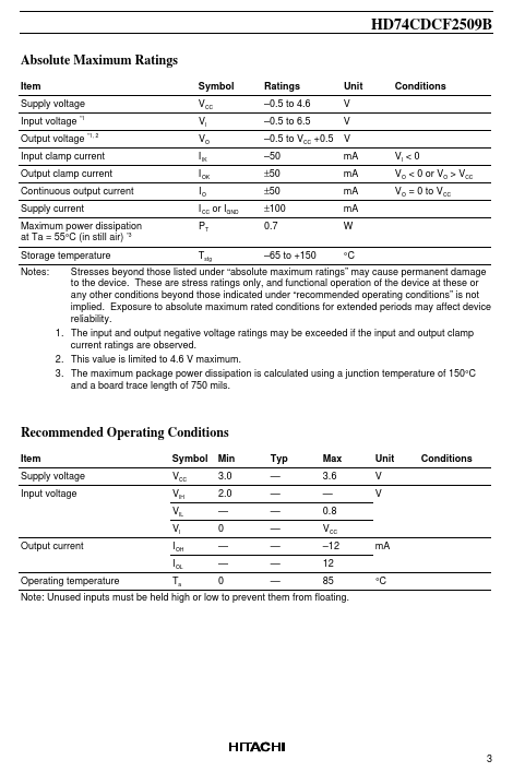
ronous DRAM.

📥 Download Datasheet

Datasheet preview – HD74CDCF2509B

Datasheet Details

Part number HD74CDCF2509B
Manufacturer Hitachi Semiconductor
File Size 41.10 KB
Description 140 MHz/ 0 to 85C Operation 3.3-V Phase-lock Loop Clock Driver
Datasheet download datasheet HD74CDCF2509B Datasheet
Additional preview pages of the HD74CDCF2509B datasheet.
Other Datasheets by Hitachi Semiconductor

Full PDF Text Transcription

Click to expand full text
HD74CDCF2509B 140 MHz, 0 to 85°C Operation 3.3-V Phase-lock Loop Clock Driver ADE-205-224F (Z) 7th. Edition January 2000 Description The HD74CDCF2509B is a high-performance, low-skew, low-jitter, phase-lock loop clock driver. It uses a phase-lock loop (PLL) to precisely align, in both frequency and phase, the feedback (FBOUT) output to the clock (CLK) input signal. It is specifically designed for use with synchronous DRAMs. The HD74CDCF2509B operates at 3.3 V VCC and is designed to drive up to five clock loads per output. One bank of five outputs and one bank of four outputs provide nine low-skew, low-jitter copies of the input clock. Output signal duty cycles are adjusted to 50 percent independent of the duty cycle at the input clock.
Published: |