HY5RS573225F Overview
and is subject to change without notice. Hynix Electronics does not assume any responsibility for use of circuits described. No patent licenses are implied.
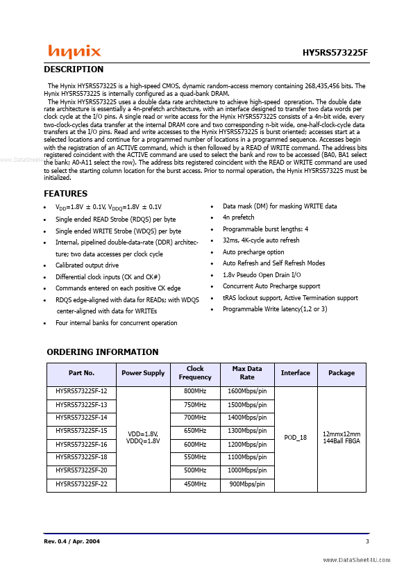
HY5RS573225F Key Features
- VDD=1.8V ± 0.1V, VDDQ=1.8V ± 0.1V Single ended READ Strobe (RDQS) per byte Single ended WRITE Strobe (WDQS) per byte Int
- Data mask (DM) for masking WRITE data 4n prefetch Programmable burst lengths: 4 32ms, 4K-cycle auto refresh Auto prechar