Datasheet4U Logo Datasheet4U.com

HY5DV641622AT - 64M(4Mx16) DDR SDRAM

Description

and is subject to change without notice.

Hynix Electronics does not assume any responsibility for use of circuits described.

No patent licenses are implied.

Features

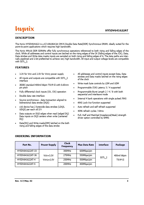
  • 3.3V for VDD and 2.5V for VDDQ power supply All inputs and outputs are compatible with SSTL_2 interface JEDEC standard 400mil 66pin TSOP-II with 0.65mm pin pitch Fully differential clock inputs (CK, /CK) operation Double data rate interface Source synchronous - data transaction aligned to bidirectional data strobe (DQS) x16 device has 2 bytewide data strobes (LDQS, UDQS) per each x8 I/O Data outputs on DQS edges when.

📥 Download Datasheet

Datasheet preview – HY5DV641622AT

Datasheet Details

Part number HY5DV641622AT
Manufacturer Hynix Semiconductor
File Size 276.42 KB
Description 64M(4Mx16) DDR SDRAM
Datasheet download datasheet HY5DV641622AT Datasheet
Additional preview pages of the HY5DV641622AT datasheet.
Other Datasheets by Hynix Semiconductor

Full PDF Text Transcription

Click to expand full text
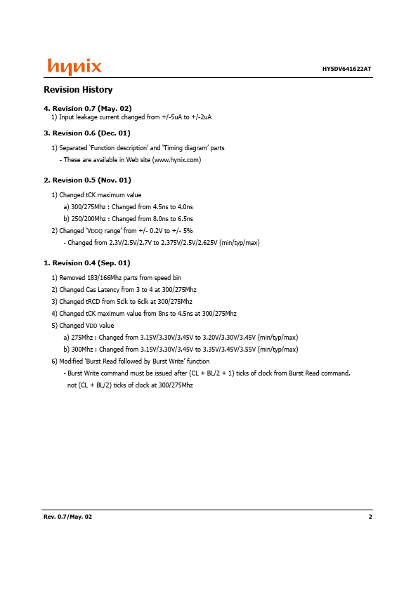
HY5DV641622AT 64M(4Mx16) DDR SDRAM HY5DV641622AT This document is a general product description and is subject to change without notice. Hynix Electronics does not assume any responsibility for use of circuits described. No patent licenses are implied. Rev. 0.7/May. 02 1 HY5DV641622AT Revision History 4. Revision 0.7 (May. 02) 1) Input leakage current changed from +/-5uA to +/-2uA 3. Revision 0.6 (Dec. 01) 1) Separated ‘Function description’ and ‘Timing diagram’ parts - These are available in Web site (www.hynix.com) 2. Revision 0.5 (Nov. 01) 1) Changed tCK maximum value a) 300/275Mhz : Changed from 4.5ns to 4.0ns b) 250/200Mhz : Changed from 8.0ns to 6.5ns 2) Changed ‘VDDQ range’ from +/- 0.2V to +/- 5% - Changed from 2.3V/2.5V/2.7V to 2.375V/2.5V/2.625V (min/typ/max) 1.
Published: |