Datasheet4U Logo Datasheet4U.com

HY5DV651622 - 4 Banks x 1M x 16Bit DOUBLE DATA RATE SDRAM

Description

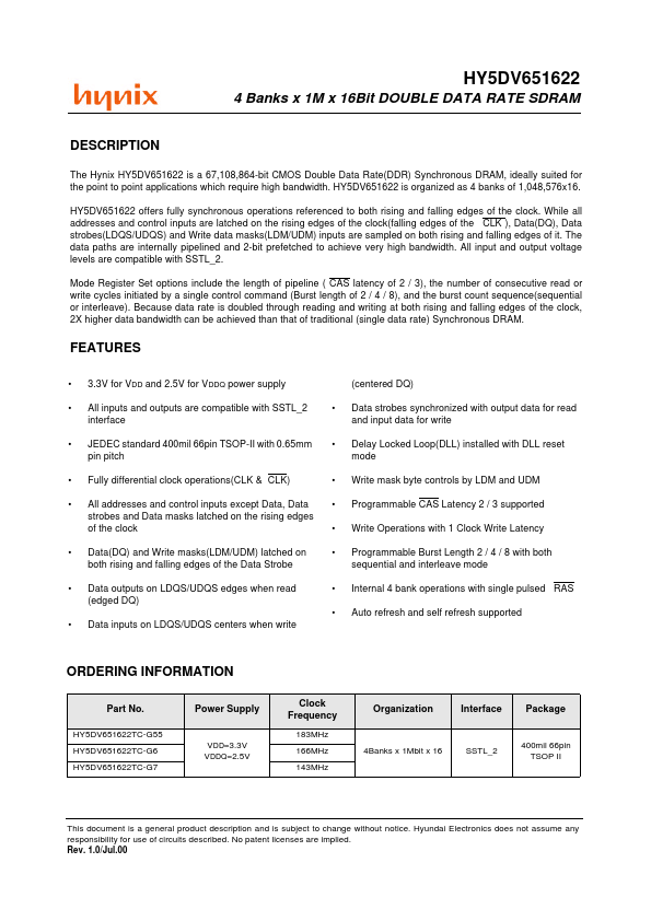
The Hynix HY5DV651622 is a 67,108,864-bit CMOS Double Data Rate(DDR) Synchronous DRAM, ideally suited for the point to point applications which require high bandwidth.

HY5DV651622 is organized as 4 banks of 1,048,576x16.

Features

  • 3.3V for VDD and 2.5V for VDDQ power supply (centered DQ).
  • All inputs and outputs are compatible with SSTL_2 interface.
  • Data strobes synchronized with output data for read and input data for write.
  • JEDEC standard 400mil 66pin TSOP-II with 0.65mm pin pitch.
  • Delay Locked Loop(DLL) installed with DLL reset mode.
  • Fully differential clock operations(CLK & CLK).
  • Write mask byte controls by LDM and UDM.
  • All addresses and.

📥 Download Datasheet

Datasheet preview – HY5DV651622

Datasheet Details

Part number HY5DV651622
Manufacturer Hynix Semiconductor
File Size 85.23 KB
Description 4 Banks x 1M x 16Bit DOUBLE DATA RATE SDRAM
Datasheet download datasheet HY5DV651622 Datasheet
Additional preview pages of the HY5DV651622 datasheet.
Other Datasheets by Hynix Semiconductor

Full PDF Text Transcription

Click to expand full text
HY5DV651622 4 Banks x 1M x 16Bit DOUBLE DATA RATE SDRAM DESCRIPTION The Hynix HY5DV651622 is a 67,108,864-bit CMOS Double Data Rate(DDR) Synchronous DRAM, ideally suited for the point to point applications which require high bandwidth. HY5DV651622 is organized as 4 banks of 1,048,576x16. HY5DV651622 offers fully synchronous operations referenced to both rising and falling edges of the clock. While all addresses and control inputs are latched on the rising edges of the clock(falling edges of the CLK ), Data(DQ), Data strobes(LDQS/UDQS) and Write data masks(LDM/UDM) inputs are sampled on both rising and falling edges of it. The data paths are internally pipelined and 2-bit prefetched to achieve very high bandwidth. All input and output voltage levels are compatible with SSTL_2.
Published: |