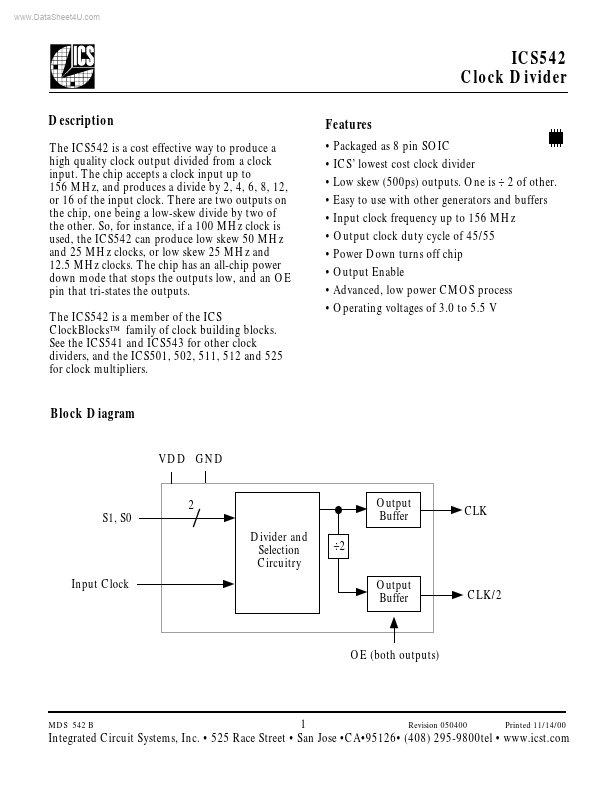
Datasheet4U Logo Datasheet4U.com

ICS542 - Clock Divider

Description

The ICS542 is a cost effective way to produce a high quality clock output divided from a clock input.

The chip accepts a clock input up to 156 MHz, and produces a divide by 2, 4, 6, 8, 12, or 16 of the input clock.

There are two outputs on the chip, one being a low-skew divide by two of the other.

Features

  • Packaged as 8 pin SOIC.
  • ICS’ lowest cost clock divider.
  • Low skew (500ps) outputs. One is ÷ 2 of other.
  • Easy to use with other generators and buffers.
  • Input clock frequency up to 156 MHz.
  • Output clock duty cycle of 45/55.
  • Power Down turns off chip.
  • Output Enable.
  • Advanced, low power CMOS process.
  • Operating voltages of 3.0 to 5.5 V Block Diagram VDD GND 2 S1, S0 Divider and Selection Circuitry Input Clock.

📥 Download Datasheet

Datasheet preview – ICS542

Datasheet Details

Part number ICS542
Manufacturer ICST
File Size 76.44 KB
Description Clock Divider
Datasheet download datasheet ICS542 Datasheet
Additional preview pages of the ICS542 datasheet.
Other Datasheets by ICST

Full PDF Text Transcription

Click to expand full text
www.DataSheet4U.com ICS542 Clock Divider Description The ICS542 is a cost effective way to produce a high quality clock output divided from a clock input. The chip accepts a clock input up to 156 MHz, and produces a divide by 2, 4, 6, 8, 12, or 16 of the input clock. There are two outputs on the chip, one being a low-skew divide by two of the other. So, for instance, if a 100 MHz clock is used, the ICS542 can produce low skew 50 MHz and 25 MHz clocks, or low skew 25 MHz and 12.5 MHz clocks. The chip has an all-chip power down mode that stops the outputs low, and an OE pin that tri-states the outputs. The ICS542 is a member of the ICS ClockBlocks™ family of clock building blocks.
Published: |