ICS541
Overview
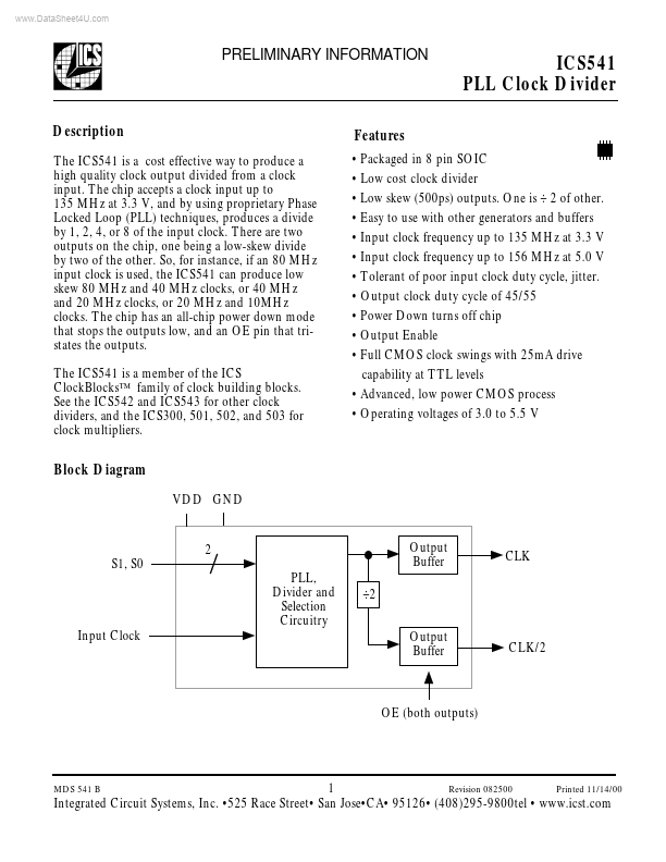
The ICS541 is a cost effective way to produce a high quality clock output divided from a clock input. The chip accepts a clock input up to 135 MHz at 3.3 V, and by using proprietary Phase Locked Loop (PLL) techniques, produces a divide by 1, 2, 4, or 8 of the input clock.
- Packaged in 8 pin SOIC
- Low cost clock divider
- Low skew (500ps) outputs. One is ÷ 2 of other.
- Easy to use with other generators and buffers
- Input clock frequency up to 135 MHz at 3.3 V
- Input clock frequency up to 156 MHz at 5.0 V
- Tolerant of poor input clock duty cycle, jitter.
- Output clock duty cycle of 45/55
- Power Down turns off chip
- Output Enable