Datasheet4U Logo Datasheet4U.com

IDT71V25781 - (IDT71V25761 / IDT71V25781) Synchronous SRAMs

Download the IDT71V25781 datasheet PDF. This datasheet also covers the IDT71V25761 variant, as both devices belong to the same (idt71v25761 / idt71v25781) synchronous srams family and are provided as variant models within a single manufacturer datasheet.

General Description

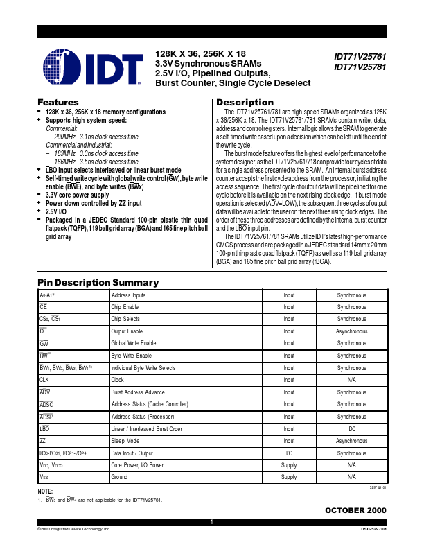
The IDT71V25761/781 are high-speed SRAMs organized as 128K x 36/256K x 18.

The IDT71V25761/781 SRAMs contain write, data, address and control registers.

Internal logic allows the SRAM to generate a self-timed write based upon a decision which can be left until the end of the write cycle.

Key Features

  • 128K x 36, 256K x 18 memory configurations Supports high system speed: Commercial:.
  • 200MHz 3.1ns clock access time Commercial and Industrial:.
  • 183MHz 3.3ns clock access time.
  • 166MHz 3.5ns clock access time LBO input selects interleaved or linear burst mode Self-timed write cycle with global write control (GW), byte write enable (BWE), and byte writes (BWx) 3.3V core power supply Power down controlled by ZZ input 2.5V I/O Packaged in a JEDEC Standard 100-pin plastic thi.

📥 Download Datasheet

Note: The manufacturer provides a single datasheet file (IDT71V25761_IDT.pdf) that lists specifications for multiple related part numbers.

Datasheet Details

Part number IDT71V25781
Manufacturer IDT
File Size 539.14 KB
Description (IDT71V25761 / IDT71V25781) Synchronous SRAMs
Datasheet download datasheet IDT71V25781 Datasheet

Full PDF Text Transcription (Reference)

The following content is an automatically extracted verbatim text from the original manufacturer datasheet and is provided for reference purposes only.

View original datasheet text
www.DataSheet4U.com 128K X 36, 256K X 18 3.3V Synchronous SRAMs 2.5V I/O, Pipelined Outputs, Burst Counter, Single Cycle Deselect x x IDT71V25761 IDT71V25781 Features 128K x 36, 256K x 18 memory configurations Supports high system speed: Commercial: – 200MHz 3.1ns clock access time Commercial and Industrial: – 183MHz 3.3ns clock access time – 166MHz 3.5ns clock access time LBO input selects interleaved or linear burst mode Self-timed write cycle with global write control (GW), byte write enable (BWE), and byte writes (BWx) 3.3V core power supply Power down controlled by ZZ input 2.