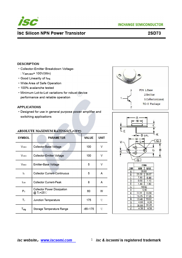
Collector-Emitter Breakdown Voltage-
: V(BR)CEO= 100V(Min)
Good Linearity of hFE
Wide Area of Safe Operation
100% avalanche tested
Minimum Lot-to-Lot variations for robust device
performance and reliable operation
APPLICATIONS
Designed for use in general purpose power a
The following content is an automatically extracted verbatim text
from the original manufacturer datasheet and is provided for reference purposes only.
View original datasheet text
isc Silicon NPN Power Transistor
INCHANGE Semiconductor
2SD73
DESCRIPTION ·Collector-Emitter Breakdown Voltage-
: V(BR)CEO= 100V(Min) ·Good Linearity of hFE ·Wide Area of Safe Operation ·100% avalanche tested ·Minimum Lot-to-Lot variations for robust device
performance and reliable operation
APPLICATIONS ·Designed for use in general purpose power amplifier and
switching applications
ABSOLUTE MAXIMUM RATINGS(Ta=25℃)
SYMBOL
PARAMETER
VALUE
UNIT
VCBO
Collector-Base Voltage
100
V
VCEO
Collector-Emitter Voltage
100
V
VEBO
Emitter-Base Voltage
5
V
IC
Collector Current-Continuous
5
A
ICM
Collector Current-Peak
PC
Collector Power Dissipation @ TC=25℃
TJ
Junction Temperature
8
A
60
W
175
℃
Tstg
Storage Temperature Range
-65~175 ℃
isc website:www.iscsemi.