ICS8543I Description
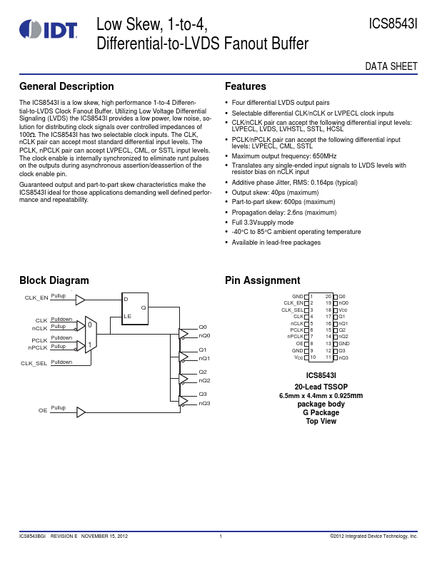
The ICS8543I is a low skew, high performance 1-to-4 Differential-to-LVDS Clock Fanout Buffer. Utilizing Low Voltage Differential Signaling (LVDS) the ICS8543I provides a low power, low noise, solution for distributing clock signals over controlled impedances of 100. The ICS8543I has two selectable clock inputs.
ICS8543I Key Features
- Four differential LVDS output pairs
- Selectable differential CLK/nCLK or LVPECL clock inputs
- CLK/nCLK pair can accept the following differential input levels
- PCLK/nPCLK pair can accept the following differential input
- Maximum output frequency: 650MHz
- Additive phase Jitter, RMS: 0.164ps (typical)
- Output skew: 40ps (maximum)
- Part-to-part skew: 600ps (maximum)
- Propagation delay: 2.6ns (maximum)
- Full 3.3Vsupply mode