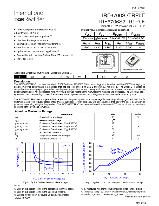
Datasheet4U Logo Datasheet4U.com

IRF6706S2TR1PBF Datasheet DirectFET Power MOSFET

Manufacturer: International Rectifier (now Infineon)

Download the IRF6706S2TR1PBF datasheet PDF. This datasheet also includes the IRF6706S2TRPBF variant, as both parts are published together in a single manufacturer document.

📥 Download Datasheet

Note: The manufacturer provides a single datasheet file (IRF6706S2TRPBF_InternationalRectifier.pdf) that lists specifications for multiple related part numbers.

General Description

The IRF6706S2TRPbF combines the latest HEXFET® Power MOSFET Silicon technology with the advanced DirectFET TM packaging to achieve improved performance in a package that has the footprint of a MICRO-8 and only 0.7 mm profile.

The DirectFET package is compatible with existing layout geometries used in power applications, PCB assembly equipment and vapor phase, infra-red or convection soldering techniques, when application note AN-1035 is followed regarding the manufacturing methods and processes.

The DirectFET package allows dual sided cooling to maximize thermal transfer in power systems, improving previous best thermal resistance by 80%.

Overview

PD - 97485 IRF6706S2TRPbF IRF6706S2TR1PbF l RoHS Compliant and Halogen Free l Low Profile (<0.7 mm) l Dual Sided Cooling Compatible l Ultra Low Package Inductance l Optimized for High Frequency Switching l Ideal for CPU Core DC-DC Converters l Optimized for Control FET Application  l Compatible with existing Surface Mount Techniques l 100% Rg tested D G S D www.DataSheet4U.com  DirectFET™ Power MOSFET ‚ Typical values (unless otherwise specified)   VDSS Qg tot VGS Qgd 4.4nC RDS(on) 3.0mΩ@10V RDS(on) 5.2mΩ@4.5V 25V max ±20V max 13nC Qgs2 1.8nC Qrr 21nC Qoss 9.5nC Vgs(th) 1.

Key Features

  • -40°C 10 10 1msec 10msec DC 1 1 VGS = 0V 0 0.1 0.2 0.3 0.4 0.5 0.6 0.7 0.8 0.9 1.0 1.1 VSD, Source-to-Drain Voltage (V) 0.1 T A = 25°C T J = 150°C Single Pulse 0.01 0.01 0.10 1.00 10.00 100.00 VDS, Drain-to-Source Voltage (V) Fig 10. Typical Source-Drain Diode Forward Voltage Typical VGS(th) Gate threshold Voltage (V) 70 60 Fig 11. Maximum Safe Operating Area 3.0 2.5 2.0 1.5 1.0 0.5 0.0 -75 -50 -25 0 25 50 75 100 125 150 175 T J , Temperature ( °C ) ID = 25µA ID = 250µA ID = 1.0mA ID.