KI30P03DFN Description
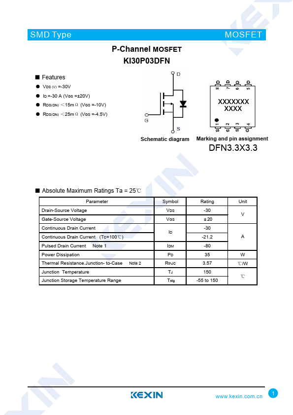
SMD Type P-Channel MOSFET KI30P03DFN.
KI30P03DFN Key Features
- VDS (V) =-30V
- ID =-30 A (VGS =±20V)
- RDS(ON) <15mΩ (VGS =-10V)
- RDS(ON) <25mΩ (VGS =-4.5V)
KI30P03DFN is P-Channel MOSFET manufactured by Kexin Semiconductor.
| Part Number | Description |
|---|---|
| KI3055 | N-Channel Enhancement MOSFET |
| KI3055DY | N-Channel MOSFET |
| KI30N03DFN | N-Channel MOSFET |
| KI3305DS | N-Channel MOSFET |
| KI3437DV | P-Channel MOSFET |
SMD Type P-Channel MOSFET KI30P03DFN.