SP332 Overview
Key Specifications
Package: SOP
Mount Type: Surface Mount
Pins: 28
Operating Voltage: 5 V
Description
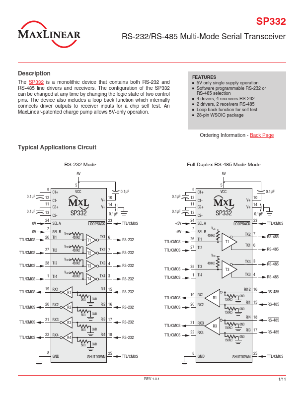
The SP332 is a monolithic device that contains both RS-232 and RS-485 line drivers and receivers. The configuration of the SP332 can be changed at any time by changing the logic state of two control pins.
Key Features
- 5V only single supply operation
- Software programmable RS-232 or RS-485 selection
- 4 drivers, 4 receivers RS-232
- 2 drivers, 2 receivers RS-485
- Loop back function for self test