MTB33N10E
Overview
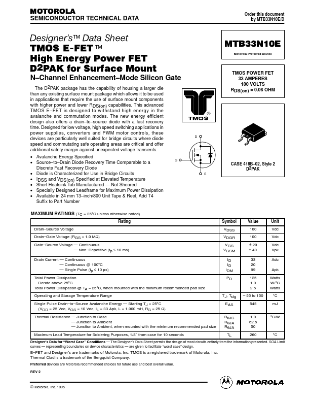
MOTOROLA SEMICONDUCTOR TECHNICAL DATA Order this document by MTB33N10E/D ™ Data Sheet TMOS E-FET.™ High Energy Power FET D2PAK for Surface Mount Designer's MTB33N10E Motorola Preferred Device N–C...
| Part | MTB33N10E |
|---|---|
| Description | TMOS POWER FET |
| Manufacturer | Motorola Semiconductor |
| Size | 266.16 KB |
MOTOROLA SEMICONDUCTOR TECHNICAL DATA Order this document by MTB33N10E/D ™ Data Sheet TMOS E-FET.™ High Energy Power FET D2PAK for Surface Mount Designer's MTB33N10E Motorola Preferred Device N–C...
| Part Number | Manufacturer | Description |
|---|---|---|
| TL074C | STMicroelectronics | LOW NOISE J-FET QUAD OPERATIONAL AMPLIFIER |
| CBT3253 | Nexperia | Dual 1-of-4 FET multiplexer/demultiplexer |
| CBT3125 | Nexperia | Quadruple FET bus switch |