2N7000
2N7000 is TMOS FET Transistor manufactured by Motorola Semiconductor.
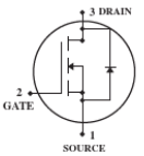
MOTOROLA
SEMICONDUCTOR TECHNICAL DATA
Order this document by 2N7000/D
TMOS FET Transistor
N- Channel
- Enhancement
3 DRAIN 2 GATE 1 SOURCE
Motorola Preferred Device
MAXIMUM RATINGS
Rating Drain Source Voltage Drain- Gate Voltage (RGS = 1.0 MΩ) Gate- Source Voltage
- Continuous
- Non- repetitive (tp ≤ 50 µs) Drain Current Continuous Pulsed Total Power Dissipation @ TC = 25°C Derate above 25°C Operating and Storage Temperature Range Symbol VDSS VDGR VGS VGSM ID IDM PD TJ, Tstg Value 60 60 ± 20 ± 40 200 500 350 2.8
- 55 to +150 m W m W/°C °C Unit Vdc Vdc Vdc Vpk m Adc CASE 29- 04, STYLE 22 TO- 92 (TO- 226AA)
1 2 3
THERMAL CHARACTERISTICS
Characteristic Thermal Resistance, Junction to Ambient Maximum Lead Temperature for Soldering Purposes, 1/16″ from case for 10 seconds Symbol RθJA TL Max 357 300 Unit °C/W °C
ELECTRICAL CHARACTERISTICS (TC = 25°C unless otherwise noted)
Characteristic Symbol Min Max Unit
OFF CHARACTERISTICS
Drain- Source Breakdown Voltage (VGS = 0, ID = 10 µAdc) Zero Gate Voltage Drain Current (VDS = 48 Vdc, VGS = 0) (VDS = 48 Vdc, VGS = 0, TJ = 125°C) Gate- Body Leakage Current, Forward (VGSF = 15 Vdc, VDS = 0) V(BR)DSS IDSS
- - IGSSF
- 1.0 1.0
- 10 60
- Vdc
µAdc m Adc n Adc
ON CHARACTERISTICS(1)
Gate Threshold Voltage (VDS = VGS, ID = 1.0 m Adc) Static Drain- Source On- Resistance (VGS = 10 Vdc, ID = 0.5 Adc) (VGS = 4.5 Vdc, ID = 75 m Adc) Drain- Source On- Voltage (VGS = 10 Vdc, ID = 0.5 Adc) (VGS = 4.5 Vdc, ID = 75 m Adc) 1. Pulse Test: Pulse Width ≤ 300 µs, Duty Cycle ≤ 2.0%.
Preferred devices are Motorola remended choices for future use and best overall value.
VGS(th) r DS(on)
Vdc Ohm
- - VDS(on)
- -
5.0 6.0 Vdc 2.5 0.45
REV 3
© Motorola, Inc. 1997
Motorola Small- Signal Transistors, FETs and Diodes Device Data
ELECTRICAL CHARACTERISTICS (TC = 25°C unless otherwise noted) (Continued)
Characteristic Symbol Min Max...
Representative 2N7000 image (package may vary by manufacturer)