logo
Datasheet4U.com - PKCK2BB
logo

PKCK2BB Datasheet, Transistor, NIKO-SEM

PKCK2BB Datasheet, Transistor, NIKO-SEM

PKCK2BB

datasheet Download (Size : 318.41KB)

PKCK2BB Datasheet
PKCK2BB

datasheet Download (Size : 318.41KB)

PKCK2BB Datasheet

PKCK2BB Features and benefits

PKCK2BB Features and benefits


* Pb−Free, Halogen Free and RoHS compliant.
* Low RDS(on) to Minimize Conduction Losses.
* Ohmic Region Good RDS(on) Ratio.
* Optimized Gate Charge to Min.

PKCK2BB Application

PKCK2BB Application


* Protection Circuits Applications.
* Computer for DC to DC Converters Applications.
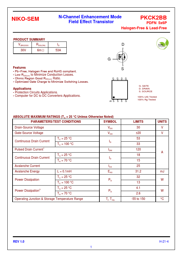
 D G S D D DD #1 S S S G .

PKCK2BB Description

PKCK2BB Description

N-Channel Enhancement Mode Field Effect Transistor

Image gallery

PKCK2BB Page 1 PKCK2BB Page 2 PKCK2BB Page 3

<?=PKCK2BB?> Page 2 <?=?> Page 3

TAGS

PKCK2BB
N-Channel
Enhancement
Mode
Field
Effect
Transistor
NIKO-SEM

Manufacturer


NIKO-SEM

Related datasheet

PKC-136

PKC136

PKC16BB

PKC2111

PKC2113

PKC26BB

PKC46DY

PKC50DY

PKCF5BB

PKCH2BB

PK0608

PK0810

PK110F

Since 2006. D4U Semicon.   |   Datasheet4U.com   |   Contact Us   |   Privacy Policy   |   Purchase of parts