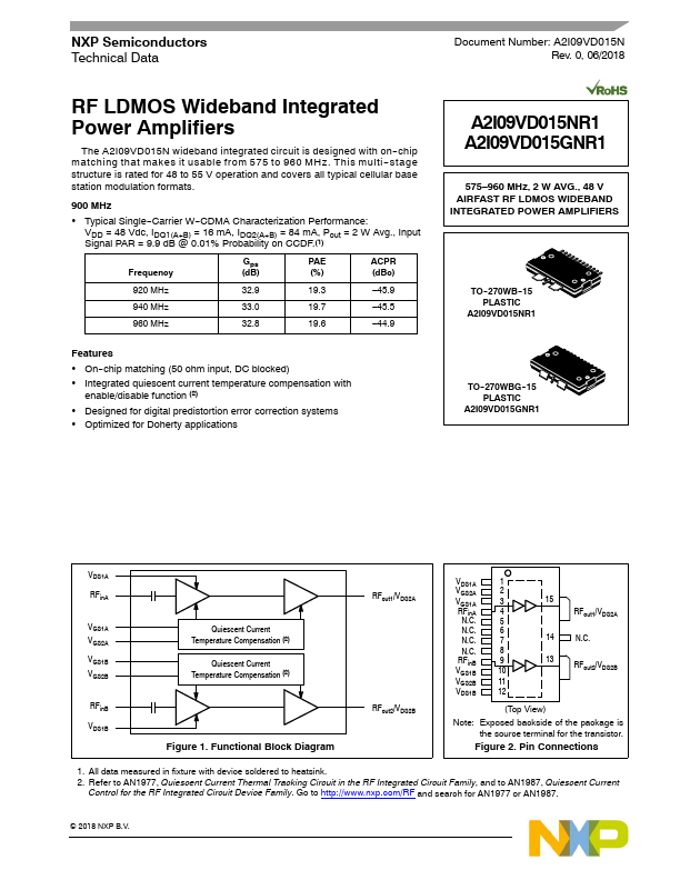
Datasheet4U Logo Datasheet4U.com

A2I09VD015GNR1 - Power Amplifiers

This page provides the datasheet information for the A2I09VD015GNR1, a member of the A2I09VD015NR1 Power Amplifiers family.

Features

  • On--chip matching (50 ohm input, DC blocked).
  • Integrated quiescent current temperature compensation with enable/disable function (2).
  • Designed for digital predistortion error correction systems.
  • Optimized for Doherty.

📥 Download Datasheet

Datasheet preview – A2I09VD015GNR1

Datasheet Details

Part number A2I09VD015GNR1
Manufacturer NXP
File Size 541.45 KB
Description Power Amplifiers
Datasheet download datasheet A2I09VD015GNR1 Datasheet
Additional preview pages of the A2I09VD015GNR1 datasheet.
Other Datasheets by NXP

Full PDF Text Transcription

Click to expand full text
NXP Semiconductors Technical Data Document Number: A2I09VD015N Rev. 0, 06/2018 RF LDMOS Wideband Integrated Power Amplifiers The A2I09VD015N wideband integrated circuit is designed with on--chip matching that makes it usable from 575 to 960 MHz. This multi -- stage structure is rated for 48 to 55 V operation and covers all typical cellular base station modulation formats. 900 MHz  Typical Single--Carrier W--CDMA Characterization Performance: VDD = 48 Vdc, IDQ1(A+B) = 16 mA, IDQ2(A+B) = 84 mA, Pout = 2 W Avg., Input Signal PAR = 9.9 dB @ 0.01% Probability on CCDF.(1) Frequency Gps (dB) PAE (%) ACPR (dBc) 920 MHz 940 MHz 960 MHz 32.9 19.3 –45.9 33.0 19.7 –45.5 32.8 19.6 –44.
Published: |