SSTUH32864 Description
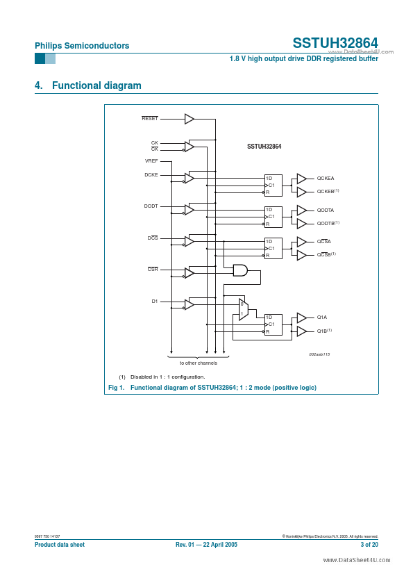
The SSTUH32864 is a 25-bit 1 : 2 configurable registered buffer designed for 1.7 V to 1.9 V VDD operation. All clock and data inputs are patible with the JEDEC standard for SSTL_18.
SSTUH32864 is 1.8 V high output drive configurable registered buffer manufactured by NXP Semiconductors.
| Part Number | Description |
|---|---|
| SSTUH32865 | 1.8V 28-bit high output drive 1:2 registered buffer |
| SSTUH32866 | 1.8 V high output drive 25-bit 1 : 1 or 14-bit 1 : 2 configurable registered buffer |
| SSTU32864 | 1.8V confgurable registered buffer |
| SSTU32865 | 28-bit 1:2 registered buffer |
| SSTU32866 | 1.8V 25-bit 1:1 or 14-bit 1:2 confgurable registered buffer |
The SSTUH32864 is a 25-bit 1 : 2 configurable registered buffer designed for 1.7 V to 1.9 V VDD operation. All clock and data inputs are patible with the JEDEC standard for SSTL_18.