SSTUH32866 Description
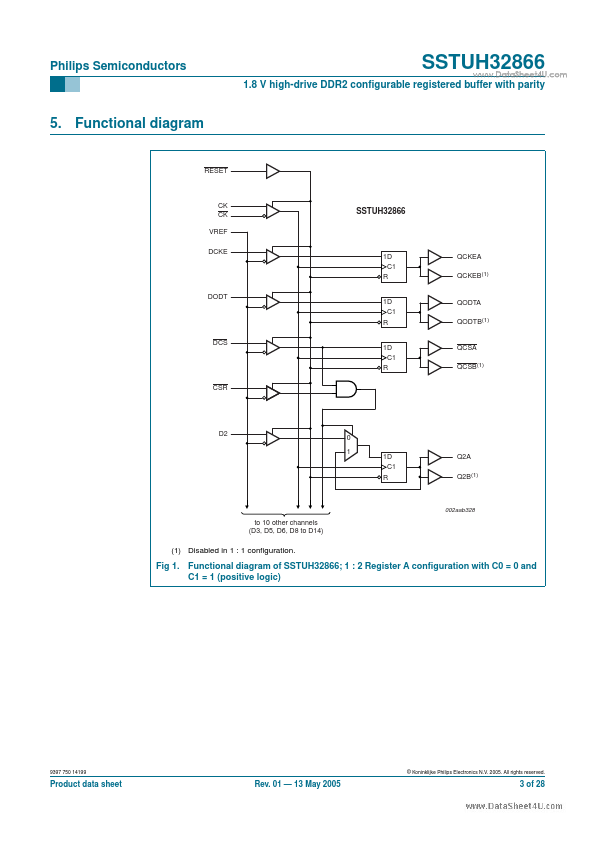
The SSTUH32866 is a 1.8 V configurable register specifically designed for use on DDR2 memory modules requiring a parity checking function. It is defined in accordance with the JEDEC JESD82-7 standard for the SSTU32864 registered buffer, while adding the parity checking function in a patible pinout. The JEDEC standard for SSTUH32866 is pending publication.