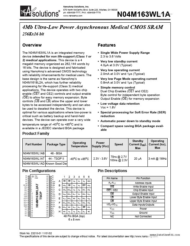
N04M163WL1A
N04M163WL1A is 4Mb Ultra-Low Power Asynchronous Medical CMOS SRAM manufactured by NanoAmp Solutions.
NanoAmp Solutions, Inc. 670 North McCarthy Blvd. Suite 220, Milpitas, CA 95035 ph: 408-935-7777, FAX: 408-935-7770 .nanoamp.
..
4Mb Ultra-Low Power Asynchronous Medical CMOS SRAM
256Kx16 bit Overview
The N04M163WL1A is an integrated memory device intended for non life-support (Class 1 or 2) medical applications. This device is a 4 megabit memory organized as 262,144 words by 16 bits. The device is designed and fabricated using NanoAmp’s advanced CMOS technology with reliability inhancements for medical users. The base design is the same as NanoAmp’s N04M1618L2A, which has further reliability processing for life-support (Class 3) medical applications....