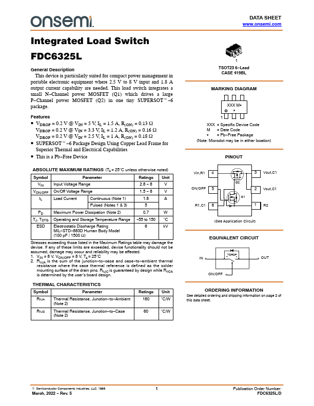
Datasheet4U Logo Datasheet4U.com

FDC6325L - Integrated Load Switch

Datasheet Summary

Description

portable electronic equipment where 2.5 V to 8 V input and 1.8 A output current capability are needed.

Channel power MOSFET (Q1) which drives a large P Channel power MOSFET (Q2) i

Features

  • VDROP = 0.2 V @ VIN = 5 V, IL = 1.5 A, R(ON) = 0.13 W VDROP = 0.2 V @ VIN = 3.3 V, IL = 1.2 A, R(ON) = 0.16 W VDROP = 0.2 V @ VIN = 2.5 V, IL = 1 A, R(ON) = 0.18 W.
  • SUPERSOTt.
  • 6 Package Design Using Copper Lead Frame for Superior Thermal and Electrical Capabilities.
  • This is a Pb.
  • Free Device.

📥 Download Datasheet

Datasheet preview – FDC6325L

Datasheet Details

Part number FDC6325L
Manufacturer ON Semiconductor
File Size 304.76 KB
Description Integrated Load Switch
Datasheet download datasheet FDC6325L Datasheet
Additional preview pages of the FDC6325L datasheet.
Other Datasheets by ON Semiconductor

Full PDF Text Transcription

Click to expand full text
Integrated Load Switch FDC6325L General Description This device is particularly suited for compact power management in portable electronic equipment where 2.5 V to 8 V input and 1.8 A output current capability are needed. This load switch integrates a small N−Channel power MOSFET (Q1) which drives a large P−Channel power MOSFET (Q2) in one tiny SUPERSOTt−6 package. Features • VDROP = 0.2 V @ VIN = 5 V, IL = 1.5 A, R(ON) = 0.13 W VDROP = 0.2 V @ VIN = 3.3 V, IL = 1.2 A, R(ON) = 0.16 W VDROP = 0.2 V @ VIN = 2.5 V, IL = 1 A, R(ON) = 0.18 W • SUPERSOTt−6 Package Design Using Copper Lead Frame for Superior Thermal and Electrical Capabilities • This is a Pb−Free Device ABSOLUTE MAXIMUM RATINGS (TA = 25°C unless otherwise noted) Symbol Parameter Ratings Unit VIN Input Voltage Range 2.
Published: |