Datasheet4U Logo Datasheet4U.com

FDC6321C

Dual N & P Channel / Digital FET

FDC6321C Features

* N-Ch 25 V, 0.68 A, RDS(ON) = 0.45 Ω @ VGS= 4.5 V P-Ch -25 V, -0.46 A, RDS(ON) = 1.1 Ω @ VGS= -4.5 V. Very low level gate drive requirements allowing direct operation in 3 V circuits. VGS(th) < 1.0V. Gate-Source Zener for ESD ruggedness. >6kV Human Body Model Replace multiple dual NPN & PNP digital t

FDC6321C General Description

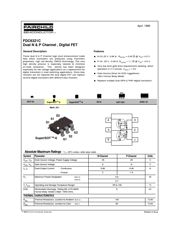
These dual N & P Channel logic level enhancement mode field effect transistors are produced using Fairchild's proprietary, high cell density, DMOS technology. This very high density process is especially tailored to minimize on-state resistance. This device has been designed especially for low volta.

FDC6321C Datasheet (273.20 KB)

Preview of FDC6321C PDF

Datasheet Details

Part number:

FDC6321C

Manufacturer:

Fairchild Semiconductor

File Size:

273.20 KB

Description:

Dual n & p channel / digital fet.

📁 Related Datasheet

FDC6321C Dual N & P-Channel Digital FET (ON Semiconductor)

FDC6320C Dual N & P Channel / Digital FET (Fairchild Semiconductor)

FDC6320C Dual N & P Channel Digital FET (ON Semiconductor)

FDC6322C Dual N & P Channel / Digital FET (Fairchild Semiconductor)

FDC6323L Integrated Load Switch (Fairchild Semiconductor)

FDC6323L Integrated Load Switch (ON Semiconductor)

FDC6324L Integrated Load Switch (Fairchild Semiconductor)

FDC6324L Integrated Load Switch (ON Semiconductor)

FDC6325L Integrated Load Switch (Fairchild Semiconductor)

FDC6325L Integrated Load Switch (ON Semiconductor)

TAGS

FDC6321C Dual Channel Digital FET Fairchild Semiconductor

Image Gallery

FDC6321C Datasheet Preview Page 2 FDC6321C Datasheet Preview Page 3

FDC6321C Distributor