Datasheet Details
| Part number | FDC6302P |
|---|---|
| Manufacturer | ON Semiconductor |
| File Size | 343.75 KB |
| Description | Dual P-Channel MOSFET |
| Datasheet |
 FDC6302P Datasheet FDC6302P Datasheet
|
|
|
| Part number | FDC6302P |
|---|---|
| Manufacturer | ON Semiconductor |
| File Size | 343.75 KB |
| Description | Dual P-Channel MOSFET |
| Datasheet |
FDC6302P Datasheet
|
|
|
|
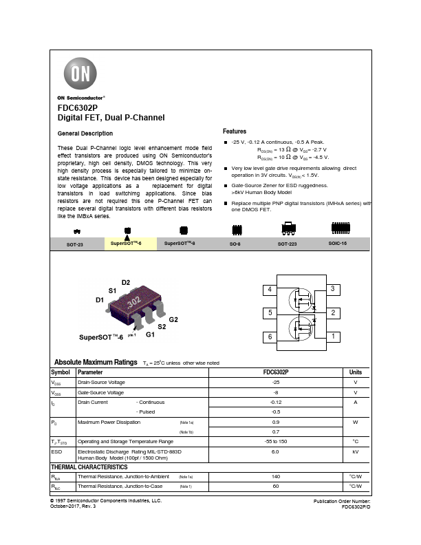
These Dual P-Channel logic level enhancement mode field effect transistors are produced using ON Semiconductor's proprietary, high cell density, DMOS technology.
📁 Similar Datasheet