Datasheet Details
| Part number | FDC6301N |
|---|---|
| Manufacturer | ON Semiconductor |
| File Size | 315.50 KB |
| Description | Dual N-Channel Digital FET |
| Datasheet |
 FDC6301N Datasheet FDC6301N Datasheet
|
|
|
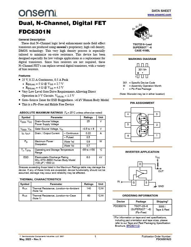
transistors are produced using onsemi’s proprietary, high cell density, DMOS technology.
state resistance.
| Part number | FDC6301N |
|---|---|
| Manufacturer | ON Semiconductor |
| File Size | 315.50 KB |
| Description | Dual N-Channel Digital FET |
| Datasheet |
FDC6301N Datasheet
|
|
|
|