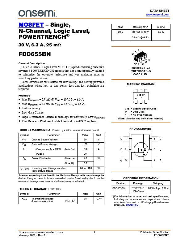
FDC655BN
Description
This N- Channel Logic Level MOSFET is produced using onsemi’s advanced POWERTRENCH process that has been especially tailored to minimize the on- state resistance and yet maintain superior switching performance.
These devices are well suited for low voltage and battery powered applications where low in- line power loss and fast switching are required.
Features
- Max RDS(ON) = 25 m W @ VGS = 10 V, ID = 6.3 A
- Max RDS(ON) = 33 m W @ VGS = 4.5 V, ID = 5.5 A
- Fast Switching
- Low Gate Charge
- High Performance Trench Technology for Extremely Low RDS(ON)
- This Device is Pb- Free, Halide Free and is Ro HS pliant
MOSFET MAXIMUM RATINGS (TC = 25°C, unless otherwise noted)
Symbol
Parameter
Value
Unit
VDS Drain to Source Voltage
VGS Gate to Source Voltage
±20
- Continuous TA = 25°C (Note 1a)
- Pulsed
PD Power Dissipation
(Note 1a)
(Note 1b)
TJ, TSTG Operating and Storage Junction Temperature Range
- 55 to +150 °C
Stresses exceeding...