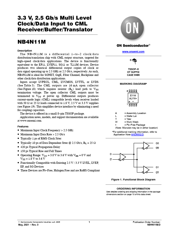
Datasheet4U Logo Datasheet4U.com

NB4N11M Datasheet - ON Semiconductor

Multi Level Clock/Data Input to CML Receiver/Buffer/Translator

NB4N11M Features

* Maximum Input Clock Frequency > 2.5 GHz

* Maximum Input Data Rate > 2.5 Gb/s

* Typically 1 ps of RMS Clock Jitter

* Typically 10 ps of Data Dependent Jitter @ 2.5 Gb/s, RL = 25 W

* 420 ps Typical Propagation Delay

* 150 ps Typical Rise and Fall Times

NB4N11M General Description

The NB4N11M is a differential 1 *to *2 clock/data distribution/translation chip with CML output structure, targeted for high *speed clock/data applications. The device is functionally equivalent to the EP11, LVEP11, SG11 or 7L11M devices. Device produces two identical differenti.

NB4N11M Datasheet (273.37 KB)

Preview of NB4N11M PDF

Datasheet Details

Part number:

NB4N11M

Manufacturer:

ON Semiconductor ↗

File Size:

273.37 KB

Description:

Multi level clock/data input to cml receiver/buffer/translator.

📁 Related Datasheet

NB4N111K Clock Fanout Buffer (ON Semiconductor)

NB4N1158 Link Replicator (ON Semiconductor)

NB4N11S 3.3V 1:2 AnyLevel Input to LVDS Fanout Buffer /Translator (ON Semiconductor)

NB4N121K 3.3V Differential 1:21 Differential Fanout Clock Driver (ON Semiconductor)

NB4N316M AnyLevel Receiver to CML Driver/Translator (ON Semiconductor)

NB4N441 3.3V Serial Input MultiProtocol PLL Clock Synthesizer (ON Semiconductor)

NB4N507A PECL Clock Synthesizer (ON Semiconductor)

NB4N527S Dual AnyLevel to LVDS Receiver/Driver/Buffer/Translator (ON Semiconductor)

NB4N7132 Link Replicator (ON Semiconductor)

NB4N840M 3.3V 3.2Gb/s Dual Differential Clock/Data 2 x 2 Crosspoint Switch (ON Semiconductor)

TAGS

NB4N11M Multi Level Clock Data Input CML Receiver Buffer Translator ON Semiconductor

Image Gallery

NB4N11M Datasheet Preview Page 2 NB4N11M Datasheet Preview Page 3

NB4N11M Distributor