Datasheet4U Logo Datasheet4U.com

NB4N527S Datasheet - ON Semiconductor

NB4N527S - Dual AnyLevel to LVDS Receiver/Driver/Buffer/Translator

Pin Name I/O Description 1 VTD1 * 
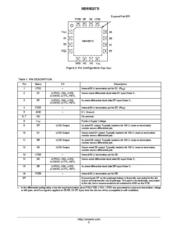
Internal 50 W termination pin for D1.

(RTIN) 2 D1 LVPECL, CML, LVDS, Noninverted differential clock/data D1 input (Note 1).

LVCMOS, LVTTL, HSTL 3 D1 LVPECL, CML, LVDS, Inverted differential clock/data D1 input (Note 1).

LVCMOS, LVTTL, HSTL 4

NB4N527S 3.3V, 2.5Gb/s Dual AnyLevelâ„¢ to LVDS Receiver/Driver/Buffer/ Translator with Internal Input Termination NB4N527S is a clock or data Receiver/Driver/Buffer/Translator capable of translating AnyLevelTM input signal (LVPECL, CML, HSTL, LVDS, or LVTTL/LVCMOS) to LVDS.

Depending on the distance, noise immunity of the system design, and transmission line media, this device will receive, drive or translate data or clock signals up to 2.5 Gb/s or 1.5 GHz, respectively.

The NB4N527S has a wide

NB4N527S_ONSemiconductor.pdf

Preview of NB4N527S PDF
NB4N527S Datasheet Preview Page 2 NB4N527S Datasheet Preview Page 3

Datasheet Details

Part number:

NB4N527S

Manufacturer:

ON Semiconductor ↗

File Size:

175.99 KB

Description:

Dual anylevel to lvds receiver/driver/buffer/translator.

📁 Related Datasheet

📌 All Tags