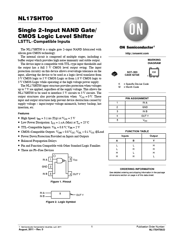
• Part: NL17SHT00
  • Description: Single 2-Input NAND Gate/CMOS Logic Level Shifter
  • Manufacturer: onsemi
  • Size: 93.72 KB
Download NL17SHT00 Datasheet PDF
onsemi
NL17SHT00
Features - High Speed: t PD = 3.1 ns (Typ) at VCC = 5 V - Low Power Dissipation: ICC = 1 m A (Max) at TA = 25°C - TTL- patible Inputs: VIL = 0.8 V; VIH = 2 V - CMOS- patible Outputs: VOH > 0.8 VCC; VOL < 0.1 VCC @Load - Power Down Protection Provided on Inputs and Outputs - Balanced Propagation Delays - Pin and Function patible with Other Standard Logic Families - These are Pb- Free Devices IN A 1 GND 2 5 VCC IN B 3 4 OUT Y Figure 1. Pinout http://onsemi. MARKING DIAGRAM SOT- 953 CASE 527AE KM 1 K = Specific Device Code M = Month Code PIN ASSIGNMENT 1 IN A 2 GND 3 IN B 4 OUT Y 5 VCC FUNCTION TABLE Inputs Output LL LH HL HH ORDERING INFORMATION See detailed ordering and shipping information in the package dimensions section on page 4 of this data sheet. IN A & IN B OUT Y Figure 2. Logic Symbol © Semiconductor ponents Industries, LLC, 2011 August, 2011 - Rev. 0 Publication Order Number: NL17SHT00/D MAXIMUM RATINGS Symbol Characteristics Val...