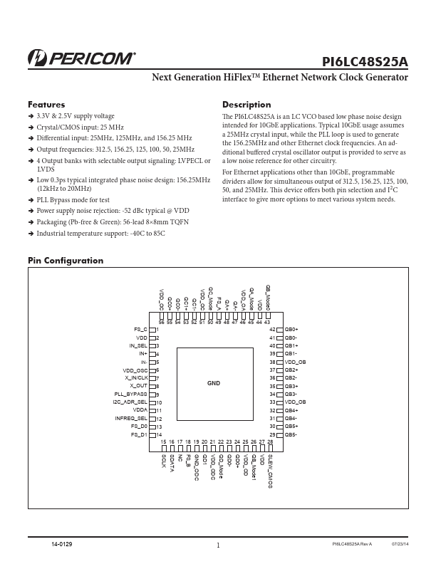
Datasheet4U Logo Datasheet4U.com

PI6LC48S25A - Ethernet Network Clock Generator

Description

The PI6LC48S25A is an LC VCO based low phase noise design intended for 10GbE applications.

Typical 10GbE usage assumes a 25MHz crystal input, while the PLL loop is used to generate the 156.25MHz and other Ethernet clock frequencies.

Features

  • ÎÎ3.3V & 2.5V supply voltage ÎÎCrystal/CMOS input: 25 MHz ÎÎDifferential input: 25MHz, 125MHz, and 156.25 MHz ÎÎOutput frequencies: 312.5, 156.25, 125, 100, 50, 25MHz ÎÎ4 Output banks with selectable output signaling: LVPECL or LVDS ÎÎLow 0.3ps typical integrated phase noise design: 156.25MHz (12kHz to 20MHz) ÎÎPLL Bypass mode for test ÎÎPower supply noise rejection: -52 dBc typical @ VDD ÎÎPackaging (Pb-free & Green): 56-lead 8×8mm TQFN ÎÎIndustrial temperature support: -40C to 85C.

📥 Download Datasheet

Datasheet preview – PI6LC48S25A

Datasheet Details

Part number PI6LC48S25A
Manufacturer Pericom Semiconductor
File Size 665.90 KB
Description Ethernet Network Clock Generator
Datasheet download datasheet PI6LC48S25A Datasheet
Additional preview pages of the PI6LC48S25A datasheet.
Other Datasheets by Pericom Semiconductor

Full PDF Text Transcription

Click to expand full text
PI6LC48S25A Next Generation HiFlexTM Ethernet Network Clock Generator Features ÎÎ3.3V & 2.5V supply voltage ÎÎCrystal/CMOS input: 25 MHz ÎÎDifferential input: 25MHz, 125MHz, and 156.25 MHz ÎÎOutput frequencies: 312.5, 156.25, 125, 100, 50, 25MHz ÎÎ4 Output banks with selectable output signaling: LVPECL or LVDS ÎÎLow 0.3ps typical integrated phase noise design: 156.25MHz (12kHz to 20MHz) ÎÎPLL Bypass mode for test ÎÎPower supply noise rejection: -52 dBc typical @ VDD ÎÎPackaging (Pb-free & Green): 56-lead 8×8mm TQFN ÎÎIndustrial temperature support: -40C to 85C Description The PI6LC48S25A is an LC VCO based low phase noise design intended for 10GbE applications. Typical 10GbE usage assumes a 25MHz crystal input, while the PLL loop is used to generate the 156.
Published: |