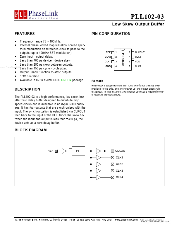
Datasheet4U Logo Datasheet4U.com

PLL102-03 - Low Skew Output Buffer

Datasheet Summary

Description

The PLL102-03 is a high performance, low skew, low jitter zero delay buffer designed to distribute high speed clocks and is available in an 8-pin SOIC package.

It has four outputs that are synchronized with the input.

The synchronization is established via CLKOUT feed back to the input of the PLL.

Features

  • Frequency range 75 ~ 180MHz. Internal phase locked loop will allow spread spectrum modulation on reference clock to pass to the outputs (up to 100kHz SST modulation).
  • Zero input - output delay.
  • Less than 700 ps device - device skew.
  • Less than 250 ps skew between outputs. www. DataSheet4U. com.
  • Less than 150 ps cycle - cycle jitter.
  • Output Enable function tri-state outputs.
  • 3.3V operation.
  • Available in 8-Pin 150mil SOIC GREEN pack.

📥 Download Datasheet

Datasheet preview – PLL102-03

Datasheet Details

Part number PLL102-03
Manufacturer PhaseLink Corporation
File Size 239.05 KB
Description Low Skew Output Buffer
Datasheet download datasheet PLL102-03 Datasheet
Additional preview pages of the PLL102-03 datasheet.
Other Datasheets by PhaseLink Corporation

Full PDF Text Transcription

Click to expand full text
PLL102-03 Low Skew Output Buffer FEATURES Frequency range 75 ~ 180MHz. Internal phase locked loop will allow spread spectrum modulation on reference clock to pass to the outputs (up to 100kHz SST modulation). • Zero input - output delay. • Less than 700 ps device - device skew. • Less than 250 ps skew between outputs. www.DataSheet4U.com • Less than 150 ps cycle - cycle jitter. • Output Enable function tri-state outputs. • 3.3V operation. • Available in 8-Pin 150mil SOIC GREEN package. • • PIN CONFIGURATION REF CLK2 CLK1 GND 1 2 3 4 8 7 6 5 CLKOUT CLK4 VDD CLK3 PLL102-03 Remark If REF clock is stopped for more than 10us after it has already been provided to the chip, and after power-up, the output clocks will disappear.
Published: |