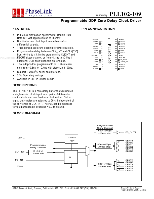
Datasheet4U Logo Datasheet4U.com

PLL102-109 - Programmable DDR Zero Delay Clock Driver

General Description

The PLL102-109 is a zero delay buffer that distributes a single-ended clock input to six pairs of differential clock outputs and one feedback clock output.

Output signal duty cycles are adjusted to 50%, independent of the duty cycle at CLK_INT.

Key Features

  • PLL clock distribution optimized for Double Data Rate SDRAM.

📥 Download Datasheet

Datasheet Details

Part number PLL102-109
Manufacturer PhaseLink Corporation
File Size 199.76 KB
Description Programmable DDR Zero Delay Clock Driver
Datasheet download datasheet PLL102-109 Datasheet

Full PDF Text Transcription (Reference)

The following content is an automatically extracted verbatim text from the original manufacturer datasheet and is provided for reference purposes only.

View original datasheet text
Preliminary PLL102-109 Programmable DDR Zero Delay Clock Driver FEATURES PLL clock distribution optimized for Double Data Rate SDRAM application up to 266Mhz. • Distributes one clock Input to one bank of six differential outputs. • Track spread spectrum clocking for EMI reduction. • Programmable delay between CLK_INT and CLK[T/C] from –0.8ns to +3.1ns by programming CLKINT and www.DataSheet4U.com FBOUT skew channel, or from –1.1ns to +3.5ns if additional DDR skew channels are enabled. • Two independent programmable DDR skew channels from –0.3ns to +0.4ns with step size ± 100ps. • Support 2-wire I 2 C serial bus interface. • • 2.5V Operating Voltage. Available in 28-Pin 209mil SSOP.