Datasheet Summary
Low Skew Output Buffer
Features
Frequency range 25 ~ 60MHz. Internal phase locked loop will allow spread spec trum modulation on reference clock to pass to the outputs (up to 33kHz SST modulation).
- Zero input
- output delay.
- Less than 700 ps device
- device skew.
- Less than 250 ps skew between outputs. ..
- Less than 200 ps cycle
- cycle jitter.
- Output Enable function tri -state outputs.
- 3.3V operation.
- Available in 8 -Pin 150mil SOIC.
- -
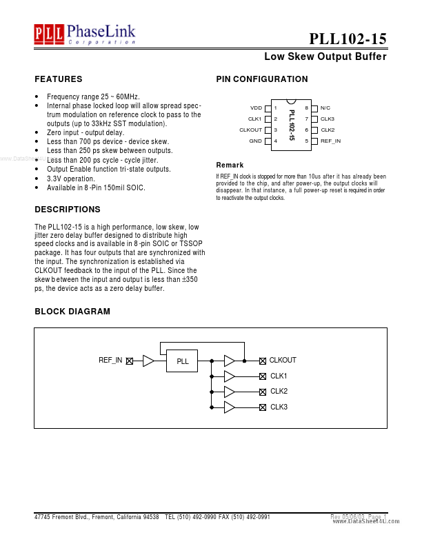
PIN CONFIGURATION
VDD CLK1 CLKOUT GND
1 2 3 4
8 7 6 5
N/C CLK3 CLK2 REF_IN
Remark
If REF_IN clock is stopped for more than 10us after it has already been provided to the chip, and after power-up, the...