PJM03N10SQ Key Features
- VDS = 100V, ID = 3A
- RDS(ON) < 140 mΩ (@VGS=10V)
- MSL: 1 Level
PJM03N10SQ is N-Channel MOSFET manufactured by Ping Jing.
| Part Number | Description |
|---|---|
| PJM10C30PA | N and P-Channel Complementary Power MOSFET |
| PJM10H05NST | N-MOS |
| PJM10H10NTE | N-Channel Enhancement Mode Power MOSFET |
| PJM2300NSA | N-Channel MOSFET |
| PJM2305PSA | P-Channel Power MOSFET |
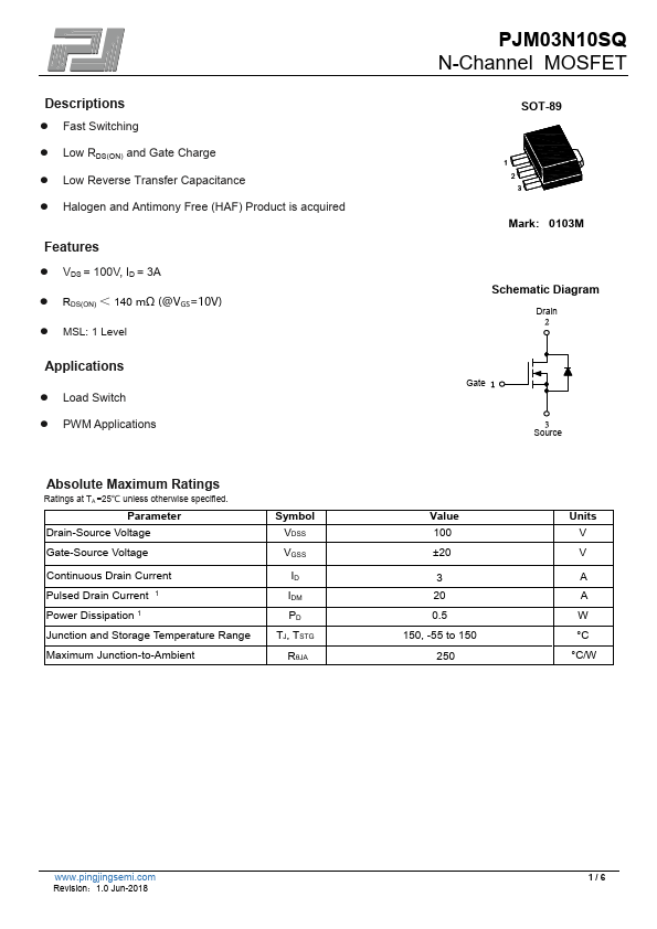
Descriptions Fast Switching Low RDS(ON) and Gate Charge Low Reverse Transfer Capacitance Halogen and Antimony Free (HAF) Product is acquired.