PJM3402NSA Key Features
- Fast Switching
- Low RDS(ON) and Gate Charge
- Low Reverse Transfer Capacitance
PJM3402NSA is N-Channel MOSFET manufactured by Ping Jing.
| Part Number | Description |
|---|---|
| PJM03N10SQ | N-Channel MOSFET |
| PJM10C30PA | N and P-Channel Complementary Power MOSFET |
| PJM10H05NST | N-MOS |
| PJM10H10NTE | N-Channel Enhancement Mode Power MOSFET |
| PJM2300NSA | N-Channel MOSFET |
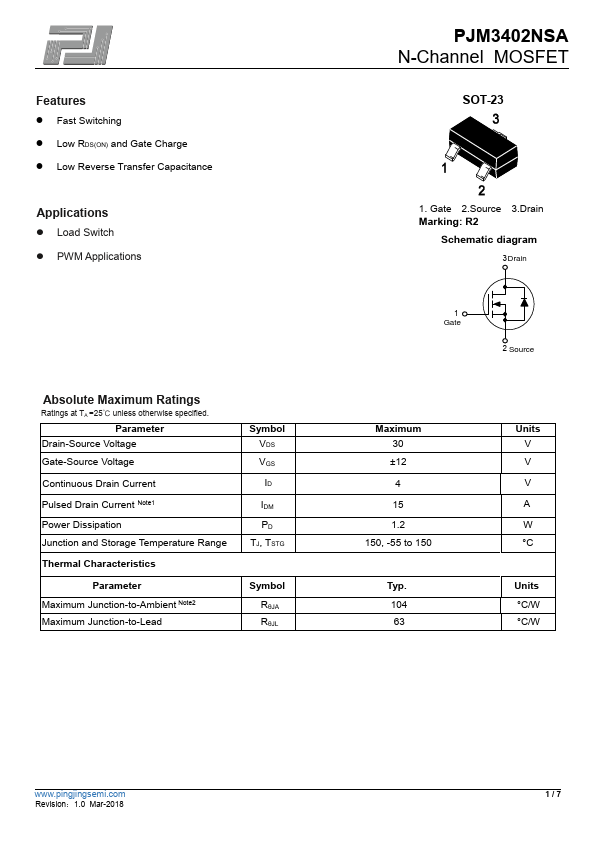
Features Fast Switching Low RDS(ON) and Gate Charge Low Reverse Transfer Capacitance Applications Load Switch PWM Applications Ratings Ratings at TA =25℃ unless otherwise specified. Parameter Drain-Source Voltage Gate-Source Voltage Continuous Drain Current Pulsed Drain Current Note1 Power Dissipation Junction and Storage Temperature Range Thermal Characteristics Parameter Maximum Junction-to-Ambient Note2 Maximum...