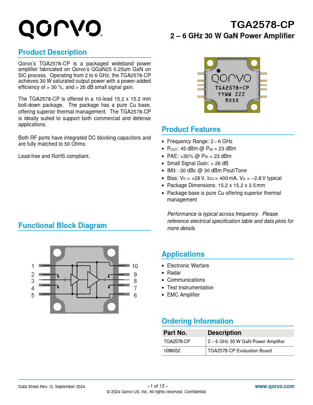
TGA2578-CP
2 – 6 GHz 30 W GaN Power Amplifier
Absolute Maximum Ratings
Parameter
Drain Voltage (VD)
Gate Voltage Range (VG)
Drain Current (ID)
Value / Range
40 V
−8 to 0 V
5 A
Gate Current (IG)
Power Dissipation (PDISS), 85°C
Input Power (PIN), 50Ω, 85°C, CW
Input Power (PIN), 85°C, VSWR 3:1,
VD = 28V, CW
Input Power (PIN), 85°C, VSWR 10:1,
VD = 28V, CW
Lead Soldering Temperature
(30 Seconds)
Storage Temperature
See plot page 8
85 W
27 dBm
27 dBm
25 dBm
260 ºC
−55 to 150 ºC
Operation of this device outside the parameter ranges given
above may cause permanent damage. These are stress ratings
only, and functional operation of the device at these conditions is
not implied.
Recommended Operating Conditions
Parameter
Min Typ. Max Units
Drain Voltage (VD)
+28 V
Drain Current, (IDQ)
400 mA
Gate Voltage (VG)
-2.8 Typical
V
TBASE Range
−40 +85 ºC
Electrical specifications are measured at specified test
conditions. Specifications are not guaranteed over all
recommended operating conditions.
Electrical Specifications
Parameter
Operational Frequency Range
Small Signal Gain
Input Return Loss
Output Return Loss
Output Power (@ PIN = 23 dBm)
Power Added Efficiency (@ PIN = 23 dBm)
IM3 (Pout/tone = 30 dBm/Tone)
IM5 (Pout/tone = 30 dBm/Tone)
Small Signal Gain Temperature Coefficient
Output Power Temperature Coefficient
Min
2
Typ
>26
>12
>5
45
>30
-30
-40
−0.05
-0.02
Test conditions unless otherwise noted: 25 ºC, VD = +28 V, IDQ = 400 mA, VG = −2.8 V typical, CW.
Max
6
Units
GHz
dB
dB
dB
dBm
%
dBc
dBc
dB/°C
dBm/°C
Data Sheet Rev. D, March 18, 2019
- 2 of 13 -
www.qorvo.com