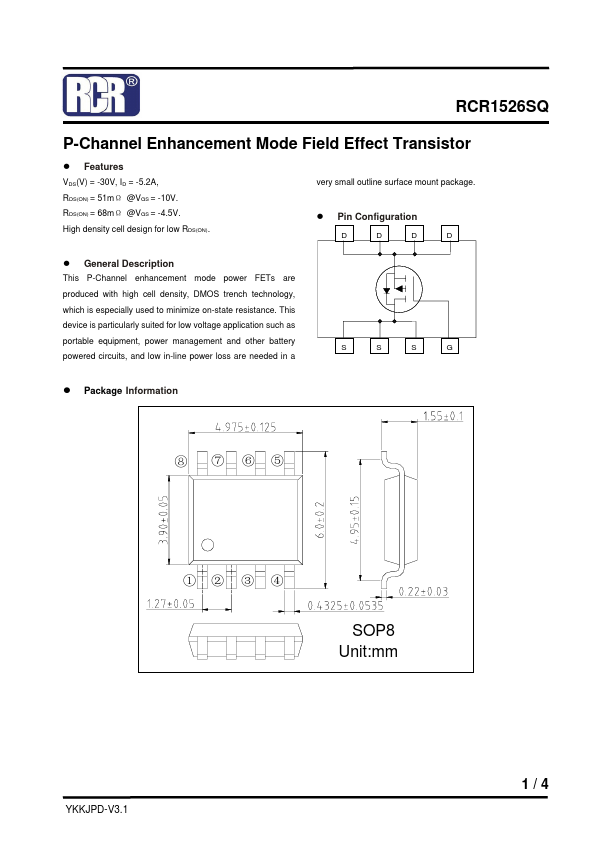
Datasheet4U Logo Datasheet4U.com

RCR1526SQ Datasheet P-Channel Enhancement Mode Field Effect Transistor

Manufacturer: RCR

Datasheet Details

Part number RCR1526SQ
Manufacturer RCR
File Size 99.06 KB
Description P-Channel Enhancement Mode Field Effect Transistor
Datasheet download datasheet RCR1526SQ Datasheet

General Description

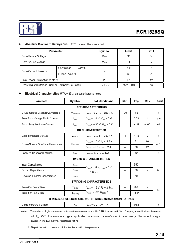
This P-Channel enhancement mode power FETs are produced with high cell density, DMOS trench technology, which is especially used to minimize on-state resistance.

This device is particularly suited for low voltage application such as portable equipment, power management and other battery powered circuits, and low in-line power loss are needed in a SSSG z Package Information ⑧ ⑦ ⑥⑤ ①② ③④ SOP8 Unit:mm YKKJPD-V3.1 1/4 RCR1526SQ z Absolute Maximum Ratings @TA = 25℃ unless otherwise noted Parameter Drain-Source Voltage Gate-Source Voltage Drain Current (Note 1) Continuous TA=25°C Pulsed (Note 2) Total Power Dissipation (Note 1) Operating and Storage Junction Temperature Range Symbol VDSS VGSS ID PD TJ, TSTG Limit -30 ±20 -5.2 -50 1.5 -55 to +150 Unit V V A A W °C z Electrical Characteristics @TA = 25℃ unless otherwise noted Parameter Symbol Test Conditions Min Typ Max Unit Drain–Source Breakdown Voltage Zero Gate Voltage Drain Current Gate–Body Leakage Current Gate Threshold Voltage Drain–Source On–State Resistance Forward Transconductance OFF CHARACTERISTICS V(BR)DSS VGS = 0 V, ID = -250μA IDSS VDS = -24 V, VGS = 0 V IGSS VGS = ± 20 V, VDS = 0 V ON CHARACTERISTICS VGS(TH) VDS = VGS, ID =-250μA RDS(ON) VGS = -10 V, ID = -4.6 A VGS = -4.5 V, ID = -2 A GFS VDS = -5 V, ID = -6 A DYNAMIC CHARACTERISTICS -30 -36 -- V -- 0.02 -1 μA -- ±1.5 ±100 nA -1 -1.46 -3 V -- 51 60 mΩ -- 68 82 -- 12 -- S Input Capacitance Output Capacitance Reverse Transfer Capacitance CISS COSS CRSS VDS = -15 V, VGS = 0 V, f = 1.0 MHz SWITCHING CHARACTERISTICS -- 550 --- 60 --- 50 -- pF Turn–On Delay Time Turn–Off Delay Tim TD(ON) TD(OFF) VDS = -15 V, RL = 2.5Ω,

Overview

RCR1526SQ P-Channel Enhancement Mode Field Effect Transistor.

Key Features

  • VDS(V) = -30V, ID = -5.2A, RDS(ON) = 51mΩ @VGS = -10V. RDS(ON) = 68mΩ @VGS = -4.5V. High density cell design for low RDS(ON). very small outline surface mount package. z Pin Configuration DDD D z General.