
HD74ALVCH162827 Overview
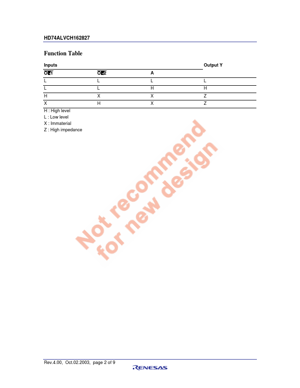
The HD74ALVCH162827 is posed of two 10-bit sections with separate output enable signals. For either 10-bit buffer section, the two output enable (1OE1 and 1OE2 or 2OE1 and 2OE2) inputs must both be low for the corresponding Y outputs to be active. If either output enable input is high, the outputs of that 10-bit buffer section are in the high impedance state.
HD74ALVCH162827 Key Features
- VCC = 2.3 V to 3.6 V
- Typical VOL ground bounce < 0.8 V (@VCC = 3.3 V, Ta = 25°C)
- Typical VOH undershoot > 2.0 V (@VCC = 3.3 V, Ta = 25°C)
- High output current ±12 mA (@VCC = 3.0 V)
- Bus hold on data inputs eliminates the need for external pullup / p