HD74HC595
Overview
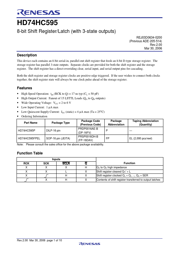
This device each contains an 8-bit serial-in, parallel-out shift register that feeds an 8-bit D-type storage register. The storage register has parallel 3-state outputs.
- High Speed Operation: tpd (RCK to Q) = 17 ns typ (CL = 50 pF)
- High Output Current: Fanout of 15 LSTTL Loads (QA to QH outputs)
- Wide Operating Voltage: VCC = 2 to 6 V
- Low Input Current: 1 µA max
- Low Quiescent Supply Current: ICC (static) = 4 µA max (Ta = 25°C)