Datasheet4U Logo Datasheet4U.com

HD74LV4066A - Quad. Analog Switches / Quad. Multiplexers

Description

The HD74LV4066A handles both analog and digital signals, and enables signals of either type with amplitudes of up to 5.5 V (peak) to be transmitted in either direction (at VCC = 0 V to 5.5 V).

Each switch section has its own enable input control (C).

Features

  • VCC = 2.0 V to 5.5 V operation.
  • All control inputs VIH (Max. ) = 5.5 V (@VCC = 0 V to 5.5 V).
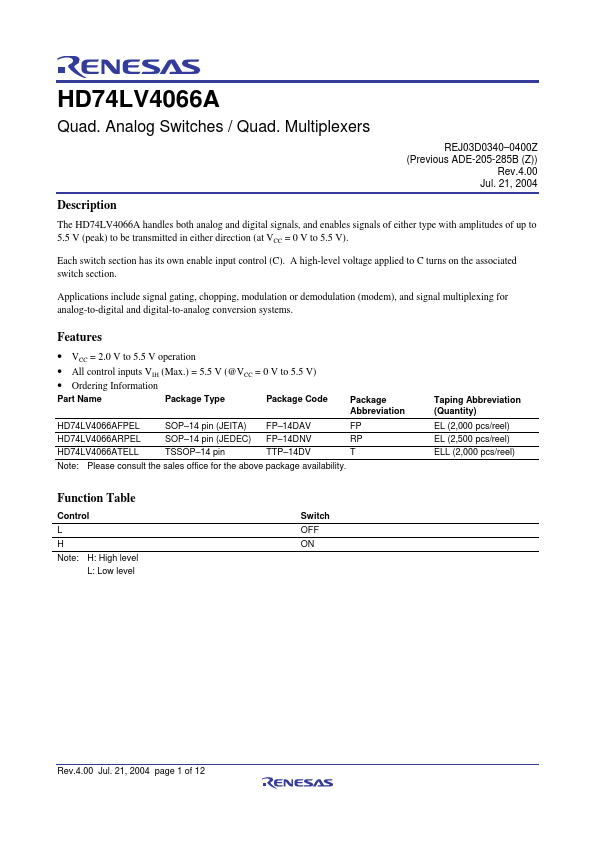
  • Ordering Information Part Name Package Type Package Code Package Abbreviation HD74LV4066AFPEL SOP.
  • 14 pin (JEITA) FP.
  • 14DAV FP HD74LV4066ARPEL SOP.
  • 14 pin (JEDEC) FP.
  • 14DNV RP HD74LV4066ATELL TSSOP.
  • 14 pin TTP.
  • 14DV T Note: Plea.

📥 Download Datasheet

Datasheet preview – HD74LV4066A

Datasheet Details

Part number HD74LV4066A
Manufacturer Renesas
File Size 116.22 KB
Description Quad. Analog Switches / Quad. Multiplexers
Datasheet download datasheet HD74LV4066A Datasheet
Additional preview pages of the HD74LV4066A datasheet.
Other Datasheets by Renesas

Full PDF Text Transcription

Click to expand full text
HD74LV4066A Quad. Analog Switches / Quad. Multiplexers REJ03D0340–0400Z (Previous ADE-205-285B (Z)) Rev.4.00 Jul. 21, 2004 Description The HD74LV4066A handles both analog and digital signals, and enables signals of either type with amplitudes of up to 5.5 V (peak) to be transmitted in either direction (at VCC = 0 V to 5.5 V). Each switch section has its own enable input control (C). A high-level voltage applied to C turns on the associated switch section. Applications include signal gating, chopping, modulation or demodulation (modem), and signal multiplexing for analog-to-digital and digital-to-analog conversion systems. Features • VCC = 2.0 V to 5.5 V operation • All control inputs VIH (Max.) = 5.5 V (@VCC = 0 V to 5.
Published: |