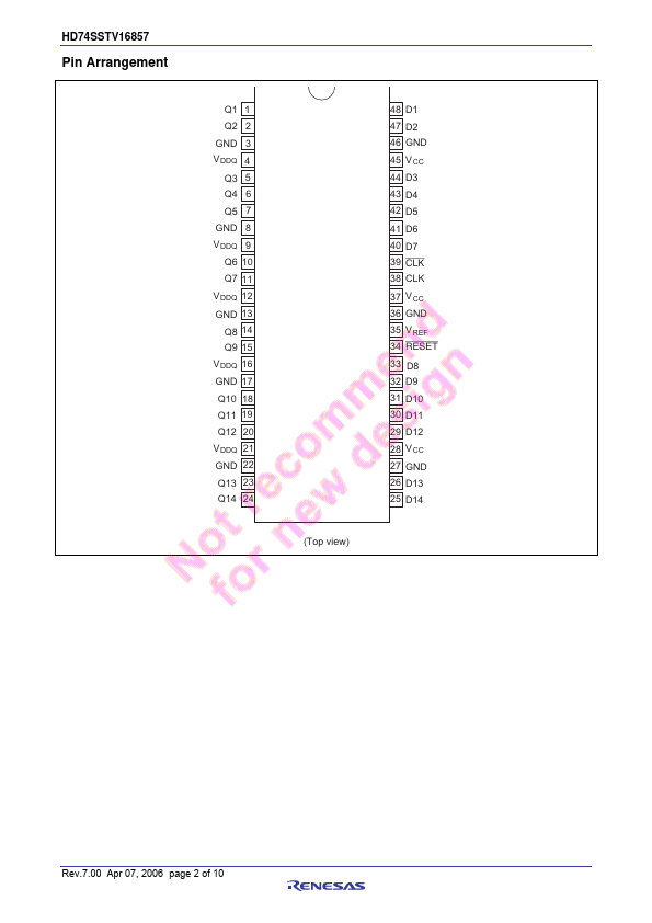
Datasheet4U Logo Datasheet4U.com

HD74SSTV16857 - 1:1 14-bit SSTL_2 Registered Buffer

Description

The HD74SSTV16857 is a 14-bit registered buffer designed for 2.3 V to 2.7 V Vcc operation and LVCMOS reset (RESET) input / SSTL_2 data (D) inputs and CLK input.

Data flow from D to Q is controlled by differential clock pins (CLK, CLK) and the RESET.

Features

  • Supports LVCMOS reset (RESET) input / SSTL_2 data (D) inputs and CLK input.
  • Differential SSTL_2 (Stub series terminated logic) CLK signal.
  • Flow through architecture optimizes PCB layout.
  • Ordering Information Part Name Package Type Package Code (Previous.

📥 Download Datasheet

Datasheet preview – HD74SSTV16857

Datasheet Details

Part number HD74SSTV16857
Manufacturer Renesas
File Size 245.03 KB
Description 1:1 14-bit SSTL_2 Registered Buffer
Datasheet download datasheet HD74SSTV16857 Datasheet
Additional preview pages of the HD74SSTV16857 datasheet.
Other Datasheets by Renesas

Full PDF Text Transcription

Click to expand full text
HD74SSTV16857 1:1 14-bit SSTL_2 Registered Buffer REJ03D0830-0700 (Previous: ADE-205-336F) Rev.7.00 Apr 07, 2006 Description The HD74SSTV16857 is a 14-bit registered buffer designed for 2.3 V to 2.7 V Vcc operation and LVCMOS reset (RESET) input / SSTL_2 data (D) inputs and CLK input. Data flow from D to Q is controlled by differential clock pins (CLK, CLK) and the RESET. Data is triggered on the positive edge of the positive clock (CLK), and the negative clock (CLK) must be used to maintain noise margins. When RESET is low, all registers are reset and all outputs are low. To ensure defined outputs from the register before a stable clock has been supplied, RESET must be held in the low state during power up.
Published: |