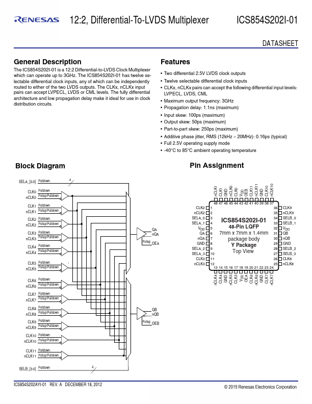
ICS854S202I-01 Description
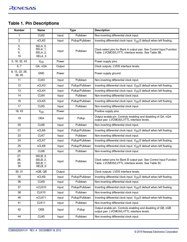
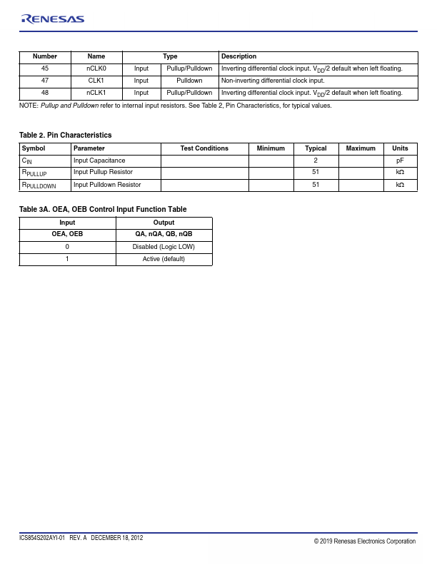
The ICS854S202I-01 is a 12:2 Differential-to-LVDS Clock Multiplexer which can operate up to 3GHz. The ICS854S202I-01 has twelve selectable differential clock inputs, any of which can be independently routed to either of the two LVDS outputs. The CLKx, nCLKx input pairs can accept LVPECL, LVDS or CML levels.
ICS854S202I-01 Key Features
- Two differential 2.5V LVDS clock outputs
- Twelve selectable differential clock inputs
- CLKx, nCLKx pairs can accept the following differential input levels
- Maximum output frequency: 3GHz
- Propagation delay: 1.1ns (maximum)
- Input skew: 100ps (maximum)
- Output skew: 50ps (maximum)
- Part-to-part skew: 250ps (maximum)
- Additive phase jitter, RMS (12kHz
- 20MHz): 0.16ps (typical)