Datasheet Summary
Two Output Differential Buffer for PCIe Gen1 & Gen2
Description
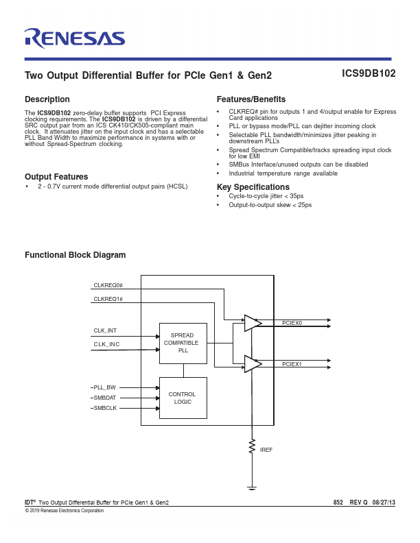
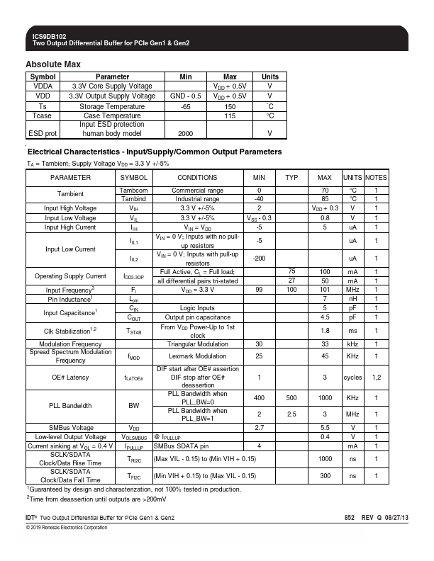
The ICS9DB102 zero-delay buffer supports PCI Express clocking requirements. The ICS9DB102 is driven by a differential SRC output pair from an ICS CK410/CK505-pliant main clock. It attenuates jitter on the input clock and has a selectable PLL Band Width to maximize performance in systems with or without Spread-Spectrum clocking.
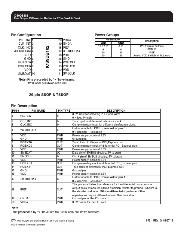
Output Features
- 2
- 0.7V current mode differential output pairs (HCSL)
Features
/Benefits
- CLKREQ# pin for outputs 1 and 4/output enable for Express Card applications
- PLL or bypass mode/PLL can dejitter ining clock
- Selectable PLL bandwidth/minimizes jitter peaking in...