M6MGT331S8BKT
M6MGT331S8BKT is CMOS SRAM manufactured by Renesas.
..
Preliminary
Notice: This is not a final specification. Some parametric limits are subject to change.
Renesas LSIs
M6MGB/T331S8BKT
33,554,432-BIT (2,097,152
- WORD BY 16-BIT /4,194,304-WORD BY 8-BIT) CMOS FLASH MEMORY & 8,388,608-BIT (524,288-WORD BY 16-BIT /1,048,576-WORD BY 8-BIT) CMOS SRAM Stacked
- µ MCP (micro Multi Chip Package)
Description
The M6MGB/T331S8BKT is a Stacked micro Multi Chip Package (S- µMCP) that contents 32M-bit Flash memory and 8M-bit Static RAM in a 52-pin TSOP for lead free use. 32M-bit Flash memory is a 4,194,304 bytes / 2,097,152 words, , single power supply and high performance nonvolatile memory fabricated by CMOS technology for the peripheral circuit and DINOR (Divided bit-line NOR IV) architecture for the memory cell. All memory blocks are locked and can not be programmed or erased, when F-WP# is low. Using Software Lock Release function, program or erase operation can be executed. 8M-bit SRAM is a 1,048,576 bytes / 524,288 words asynchronous SRAM fabricated by CMOS technology for the peripheral circuit . The M6MGB/T331S8BKT is suitable for a high performance cellular phone and a mobile PC that are required to be small mounting area, weight and small power dissipation
Features
Access Time Flash SRAM Supply Voltage Ambient Temperature Package 70ns (Max.) 85ns (Max.) VCC=2.7 ~ 3.0V Ta=-40 ~ 85 °C 52pin TSOP(Type-II), Lead pitch 0.4mm Outer-lead finishing:Sn-Cu
Application
Mobile munication products
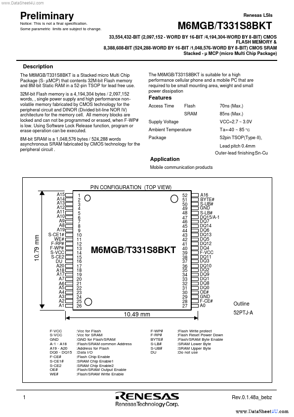
PIN CONFIGURATION (TOP VIEW)
A15 A14 A13 A12 A11 A10 A9 A8 A19 S-CE1# WE# F-RP# F-WP# S-VCC S-CE2 DU A20 A18 A17 A7 A6 A5 A4 A3 A2 A1
..
M6MGB/T331S8BKT
1 2 3 4 5 6 7 8 9 10 11 12 13 14 15 16 17 18 19 20 21 22 23 24 25 26
52 51 50 49 48 47 46 45 44 43 42 41 40 39 38 37 36 35 34 33 32 31 30 29 28 27
A16 BYTE# S-UB# GND S-LB# DQ15/A-1 DQ7 DQ14 DQ6 DQ13 DQ5 DQ12 DQ4 F-VCC DQ11 DQ3 DQ10 DQ2 DQ9 DQ1 DQ8 DQ0 OE# GND F-CE# A0
10.79 mm
Outline 52PTJ-A
10.49 mm
F-VCC S-VCC GND A-1
- A18 A19
- A20...