M25P80
SUMMARY DESCRIPTION
The M25P80 is a 8 Mbit (1M x 8) Serial Flash
Memory, with advanced write protection mecha-
nisms, accessed by a high speed SPI-compatible
bus.
The memory can be programmed 1 to 256 bytes at
a time, using the Page Program instruction.
The memory is organized as 16 sectors, each con-
taining 256 pages. Each page is 256 bytes wide.
Thus, the whole memory can be viewed as con-
sisting of 4096 pages, or 1,048,576 bytes.
The whole memory can be erased using the Bulk
Erase instruction, or a sector at a time, using the
Sector Erase instruction.
Figure 2. Logic Diagram
VCC
Figure
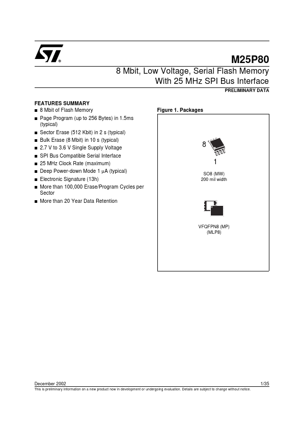
 3. SO and VFQFPN Connections
M25P80
S1
Q2
8 VCC
7 HOLD
W3
6C
VSS 4
5D
AI04965B
D
C
S
W
HOLD
M25P80
Q
Note: 1. See page 31 (onwards) for package dimensions, and how
to identify pin-1.
VSS
Table 1. Signal Names
C Serial Clock
D Serial Data Input
Q Serial Data Output
S Chip Select
W Write Protect
HOLD
Hold
VCC Supply Voltage
VSS Ground
AI04964
2/35