PSD813F1A Overview
Key Features
- DUAL BANK FLASH MEMORIES Figure
- 16 Kbit SRAM P t(s
- PLD WITH MACROCELLS te c– Over 3,000 Gates Of PLD: DPLD and le uCPLD d– DPLD
- User-defined Internal chip-select so rodecoding b P– CPLD with 16 Output Macrocells (OMCs)
- O teand 24 Input Macrocells (IMCs)
- OMCU I/Os ro )PLD I/Os P t(sLatched MCU address output; and te cSpecial function I/Os le u
- PAGE REGISTER o– Internal page register that can be used to s expand the microcontroller address space b by a factor of
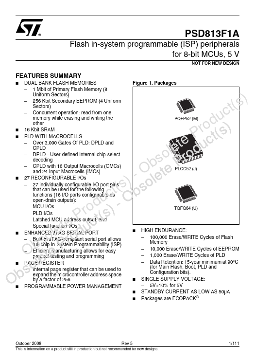
- PROGRAMMABLE POWER MANAGEMENT PQFP52 (M) PLCC52 (J) TQFQ64 (U)
- SINGLE SUPPLY VOLTAGE: – 5V±10% for 5V
- STANDBY CURRENT AS LOW AS 50µA