K3S7V2000M-TC Overview
Key Specifications
Description
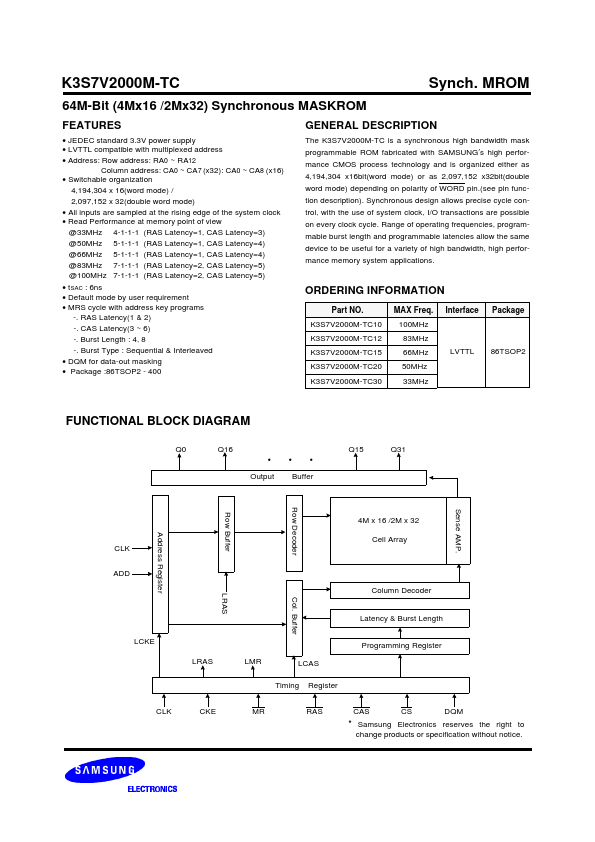
The K3S7V2000M-TC is a synchronous high bandwidth mask programmable ROM fabricated with SAMSUNG′s high performance CMOS process technology and is organized either as 4,194,304 x16bit(word mode) or as 2,097,152 x32bit(double word mode) depending on polarity of WORD pin.(see pin function description). Synchronous design allows precise cycle control, with the use of system clock, I/O transactions are possible on every clock cycle.
Key Features
- JEDEC standard 3.3V power supply
- LVTTL compatible with multiplexed address
- Address: Row address: RA0 ~ RA12 Column address: CA0 ~ CA7 (x32): CA0 ~ CA8 (x16)
- All inputs are sampled at the rising edge of the system clock
- Default mode by user requirement