Datasheet4U Logo Datasheet4U.com

SLA24C04 - 4 Kbit 512 x 8 bit Serial CMOS EEPROMs/ I2C Synchronous 2-Wire Bus/ Page Protection Mode

Description

Serial Clock (SCL) The SCL input is used to clock data into the device on the rising edge and to clock data out of the device on the falling edge.

Features

  • Data EEPROM internally organized as 512 bytes and 32 pages × 16 bytes.
  • Low power CMOS.
  • VCC = 2.7 to 5.5 V operation.
  • Two wire serial interface bus, I2C-Bus compatible.
  • Filtered inputs for noise suppression with Schmitt trigger.
  • Clock frequency up to 400 kHz.
  • High programming flexibility.
  • Internal programming voltage.
  • Self timed programming cycle including erase.
  • Byte-write and page-write programming, betwe.

📥 Download Datasheet

Datasheet preview – SLA24C04

Datasheet Details

Part number SLA24C04
Manufacturer Siemens Semiconductor Group
File Size 314.38 KB
Description 4 Kbit 512 x 8 bit Serial CMOS EEPROMs/ I2C Synchronous 2-Wire Bus/ Page Protection Mode
Datasheet download datasheet SLA24C04 Datasheet
Additional preview pages of the SLA24C04 datasheet.
Other Datasheets by Siemens Semiconductor Group

Full PDF Text Transcription

Click to expand full text
Standard EEPROM ICs 
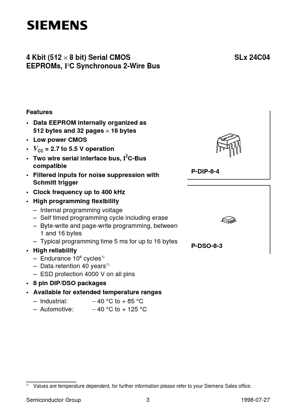
SLx 24C04 4 Kbit (512 × 8 bit) Serial CMOS-EEPROM with I2C Synchronous 2-Wire Bus Data Sheet 1998-07-27 SLx 24C04 Revision History: Previous Version: Page Page (in previous (in current Version) Version) 3 4, 5 5 5 11, 12 15 19 20 20 20 I2C Bus Current Version: 1998-07-27 06.97 Subjects (major changes since last revision) 3 4, 4 – 5 11, 12 15 19 20 20 20 Text was changed to “Typical programming time 5 ms for up to 16 bytes”. CS0, CS1 and CS2 were replaced by n.c. The paragraph “Chip Select (CS0, CS1, CS2)” was removed completely. WP = VCC protects the upper half entire memory. The erase/write cycle is finished latest after 10 8 ms. Figure 11: second command byte is a CSR and not CSW. “Capacitive load …” were added. Some timings were changed.
Published: |