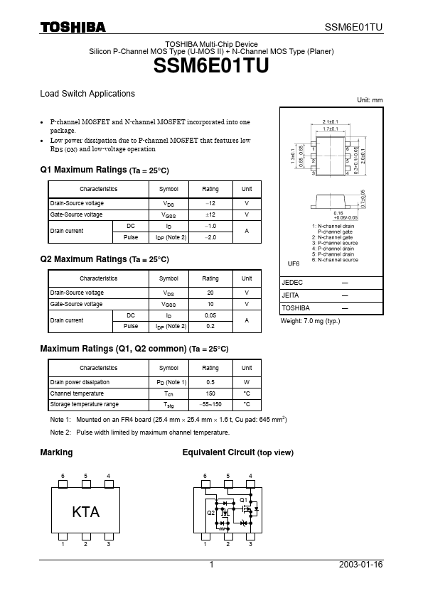
low RDS (ON) and low-voltage operation Unit: mm
Q1 Maximum Ratings (Ta = 25°C)
Characteristics Drain-Source voltage Gate-Source voltage Drain current DC Pulse Symbol VDS VGSS ID IDP (Note 2) Rating -12 ±12 -1.0 -2.0 Unit V V A
Q2 Maximum Ratings (Ta = 25°C)
Characteristics Drain-Source voltage Gate-Source voltage Drain current DC Pulse Symbol VDS VGSS ID IDP (Note 2) Rating 20 10 0.05 0.2 Unit V V A
JEDEC JEITA.
Full PDF Text Transcription for SSM6E01TU (Reference)
Note: Below is a high-fidelity text extraction (approx. 800 characters) for
SSM6E01TU. For precise diagrams, and layout, please refer to the original PDF.
SSM6E01TU TOSHIBA Multi-Chip Device Silicon P-Channel MOS Type (U-MOS II) + N-Channel MOS Type (Planer) SSM6E01TU Load Switch Applications · · P-channel MOSFET and N-chan...
View more extracted text
er) SSM6E01TU Load Switch Applications · · P-channel MOSFET and N-channel MOSFET incorporated into one package. Low power dissipation due to P-channel MOSFET that features low RDS (ON) and low-voltage operation Unit: mm Q1 Maximum Ratings (Ta = 25°C) Characteristics Drain-Source voltage Gate-Source voltage Drain current DC Pulse Symbol VDS VGSS ID IDP (Note 2) Rating -12 ±12 -1.0 -2.0 Unit V V A Q2 Maximum Ratings (Ta = 25°C) Characteristics Drain-Source voltage Gate-Source voltage Drain current DC Pulse Symbol VDS VGSS ID IDP (Note 2) Rating 20 10 0.05 0.2 Unit V V A JEDEC JEITA TOSHIBA Weight: 7.0 mg (typ.